Zihan Yin
AgentIF-OneDay: A Task-level Instruction-Following Benchmark for General AI Agents in Daily Scenarios
Jan 28, 2026Abstract:The capacity of AI agents to effectively handle tasks of increasing duration and complexity continues to grow, demonstrating exceptional performance in coding, deep research, and complex problem-solving evaluations. However, in daily scenarios, the perception of these advanced AI capabilities among general users remains limited. We argue that current evaluations prioritize increasing task difficulty without sufficiently addressing the diversity of agentic tasks necessary to cover the daily work, life, and learning activities of a broad demographic. To address this, we propose AgentIF-OneDay, aimed at determining whether general users can utilize natural language instructions and AI agents to complete a diverse array of daily tasks. These tasks require not only solving problems through dialogue but also understanding various attachment types and delivering tangible file-based results. The benchmark is structured around three user-centric categories: Open Workflow Execution, which assesses adherence to explicit and complex workflows; Latent Instruction, which requires agents to infer implicit instructions from attachments; and Iterative Refinement, which involves modifying or expanding upon ongoing work. We employ instance-level rubrics and a refined evaluation pipeline that aligns LLM-based verification with human judgment, achieving an 80.1% agreement rate using Gemini-3-Pro. AgentIF-OneDay comprises 104 tasks covering 767 scoring points. We benchmarked four leading general AI agents and found that agent products built based on APIs and ChatGPT agents based on agent RL remain in the first tier simultaneously. Leading LLM APIs and open-source models have internalized agentic capabilities, enabling AI application teams to develop cutting-edge Agent products.
xbench: Tracking Agents Productivity Scaling with Profession-Aligned Real-World Evaluations
Jun 16, 2025

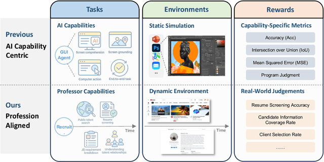
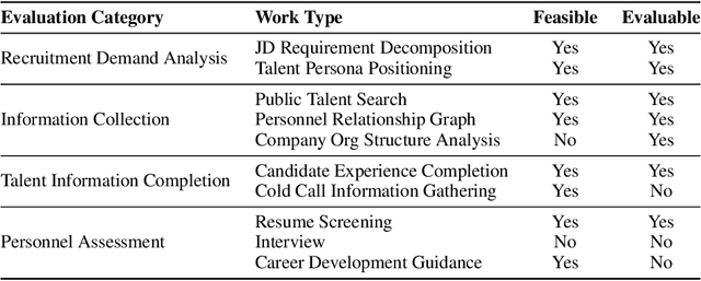
Abstract:We introduce xbench, a dynamic, profession-aligned evaluation suite designed to bridge the gap between AI agent capabilities and real-world productivity. While existing benchmarks often focus on isolated technical skills, they may not accurately reflect the economic value agents deliver in professional settings. To address this, xbench targets commercially significant domains with evaluation tasks defined by industry professionals. Our framework creates metrics that strongly correlate with productivity value, enables prediction of Technology-Market Fit (TMF), and facilitates tracking of product capabilities over time. As our initial implementations, we present two benchmarks: Recruitment and Marketing. For Recruitment, we collect 50 tasks from real-world headhunting business scenarios to evaluate agents' abilities in company mapping, information retrieval, and talent sourcing. For Marketing, we assess agents' ability to match influencers with advertiser needs, evaluating their performance across 50 advertiser requirements using a curated pool of 836 candidate influencers. We present initial evaluation results for leading contemporary agents, establishing a baseline for these professional domains. Our continuously updated evalsets and evaluations are available at https://xbench.org.
A Pathway to Near Tissue Computing through Processing-in-CTIA Pixels for Biomedical Applications
Mar 21, 2025Abstract:Near-tissue computing requires sensor-level processing of high-resolution images, essential for real-time biomedical diagnostics and surgical guidance. To address this need, we introduce a novel Capacitive Transimpedance Amplifier-based In-Pixel Computing (CTIA-IPC) architecture. Our design leverages CTIA pixels that are widely used for biomedical imaging owing to the inherent advantages of excellent linearity, low noise, and robust operation under low-light conditions. We augment CTIA pixels with IPC to enable precise deep learning computations including multi-channel, multi-bit convolution operations along with integrated batch normalization (BN) and Rectified Linear Unit (ReLU) functionalities in the peripheral ADC (Analog to Digital Converters). This design improves the linearity of Multiply and Accumulate (MAC) operations while enhancing computational efficiency. Leveraging 3D integration to embed pixel circuitry and weight storage, CTIA-IPC maintains pixel density comparable to standard CTIA designs. Moreover, our algorithm-circuit co-design approach enables efficient real-time diagnostics and AI-driven medical analysis. Evaluated on the EndoVis tissu dataset (1280x1024), CTIA-IPC achieves approximately 12x reduction in data bandwidth, yielding segmentation IoUs of 75.91% (parts), and 28.58% (instrument)-a minimal accuracy reduction (1.3%-2.5%) compared to baseline methods. Achieving 1.98 GOPS throughput and 3.39 GOPS/W efficiency, our CTIA-IPC architecture offers a promising computational framework tailored specifically for biomedical near-tissue computing.
FPCA: Field-Programmable Pixel Convolutional Array for Extreme-Edge Intelligence
Aug 03, 2024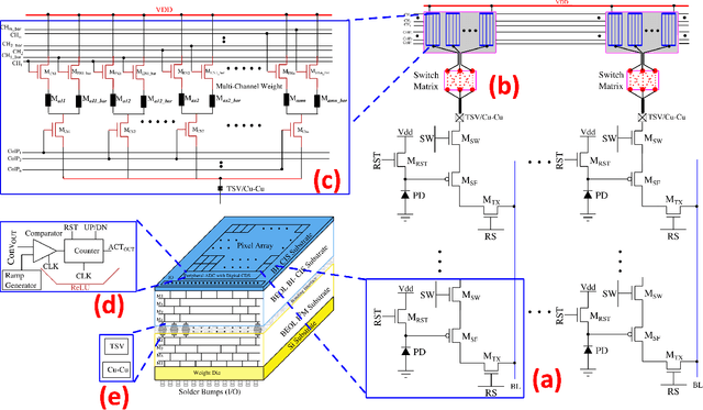
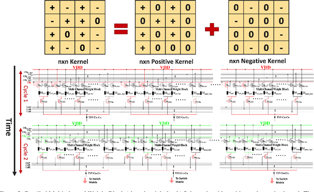
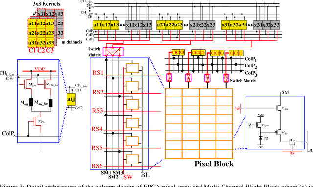

Abstract:The rapid advancement of neural network applications necessitates hardware that not only accelerates computation but also adapts efficiently to dynamic processing requirements. While processing-in-pixel has emerged as a promising solution to overcome the bottlenecks of traditional architectures at the extreme-edge, existing implementations face limitations in reconfigurability and scalability due to their static nature and inefficient area usage. Addressing these challenges, we present a novel architecture that significantly enhances the capabilities of processing-in-pixel for convolutional neural networks. Our design innovatively integrates non-volatile memory (NVM) with novel unit pixel circuit design, enabling dynamic reconfiguration of synaptic weights, kernel size, channel size and stride size. Thus offering unprecedented flexibility and adaptability. With using a separate die for pixel circuit and storing synaptic weights, our circuit achieves a substantial reduction in the required area per pixel thereby increasing the density and scalability of the pixel array. Simulation results demonstrate dot product operations of the circuit, the non-linearity of its analog output and a novel bucket-select curvefit model is proposed to capture it. This work not only addresses the limitations of current in-pixel computing approaches but also opens new avenues for developing more efficient, flexible, and scalable neural network hardware, paving the way for advanced AI applications.
Technology-Circuit-Algorithm Tri-Design for Processing-in-Pixel-in-Memory (P2M)
Apr 06, 2023


Abstract:The massive amounts of data generated by camera sensors motivate data processing inside pixel arrays, i.e., at the extreme-edge. Several critical developments have fueled recent interest in the processing-in-pixel-in-memory paradigm for a wide range of visual machine intelligence tasks, including (1) advances in 3D integration technology to enable complex processing inside each pixel in a 3D integrated manner while maintaining pixel density, (2) analog processing circuit techniques for massively parallel low-energy in-pixel computations, and (3) algorithmic techniques to mitigate non-idealities associated with analog processing through hardware-aware training schemes. This article presents a comprehensive technology-circuit-algorithm landscape that connects technology capabilities, circuit design strategies, and algorithmic optimizations to power, performance, area, bandwidth reduction, and application-level accuracy metrics. We present our results using a comprehensive co-design framework incorporating hardware and algorithmic optimizations for various complex real-life visual intelligence tasks mapped onto our P2M paradigm.
In-Sensor & Neuromorphic Computing are all you need for Energy Efficient Computer Vision
Dec 21, 2022Abstract:Due to the high activation sparsity and use of accumulates (AC) instead of expensive multiply-and-accumulates (MAC), neuromorphic spiking neural networks (SNNs) have emerged as a promising low-power alternative to traditional DNNs for several computer vision (CV) applications. However, most existing SNNs require multiple time steps for acceptable inference accuracy, hindering real-time deployment and increasing spiking activity and, consequently, energy consumption. Recent works proposed direct encoding that directly feeds the analog pixel values in the first layer of the SNN in order to significantly reduce the number of time steps. Although the overhead for the first layer MACs with direct encoding is negligible for deep SNNs and the CV processing is efficient using SNNs, the data transfer between the image sensors and the downstream processing costs significant bandwidth and may dominate the total energy. To mitigate this concern, we propose an in-sensor computing hardware-software co-design framework for SNNs targeting image recognition tasks. Our approach reduces the bandwidth between sensing and processing by 12-96x and the resulting total energy by 2.32x compared to traditional CV processing, with a 3.8% reduction in accuracy on ImageNet.
Enabling ISP-less Low-Power Computer Vision
Oct 11, 2022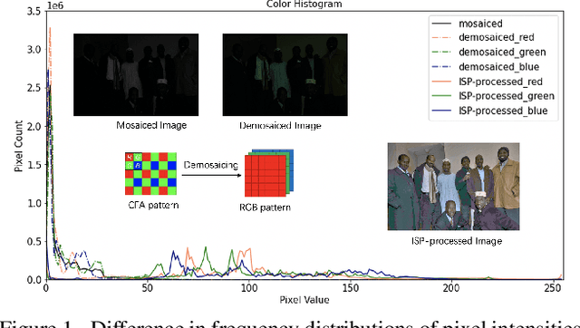
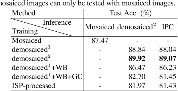
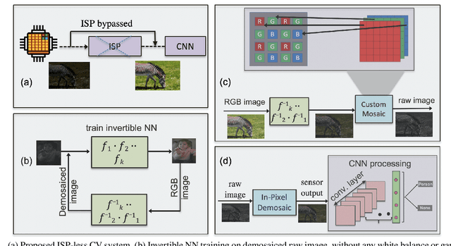
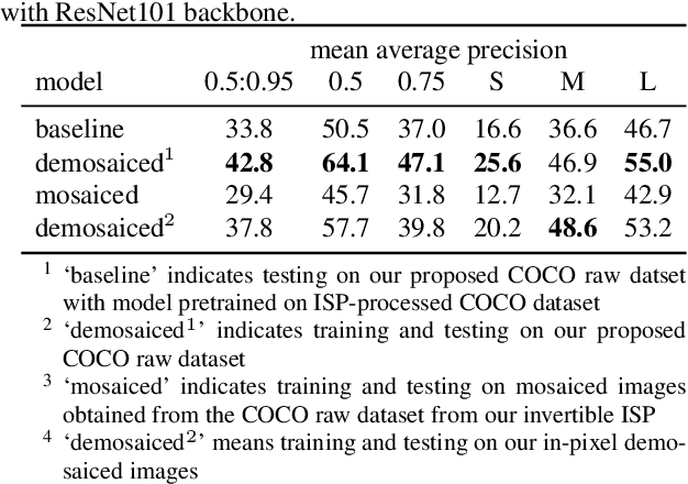
Abstract:In order to deploy current computer vision (CV) models on resource-constrained low-power devices, recent works have proposed in-sensor and in-pixel computing approaches that try to partly/fully bypass the image signal processor (ISP) and yield significant bandwidth reduction between the image sensor and the CV processing unit by downsampling the activation maps in the initial convolutional neural network (CNN) layers. However, direct inference on the raw images degrades the test accuracy due to the difference in covariance of the raw images captured by the image sensors compared to the ISP-processed images used for training. Moreover, it is difficult to train deep CV models on raw images, because most (if not all) large-scale open-source datasets consist of RGB images. To mitigate this concern, we propose to invert the ISP pipeline, which can convert the RGB images of any dataset to its raw counterparts, and enable model training on raw images. We release the raw version of the COCO dataset, a large-scale benchmark for generic high-level vision tasks. For ISP-less CV systems, training on these raw images result in a 7.1% increase in test accuracy on the visual wake works (VWW) dataset compared to relying on training with traditional ISP-processed RGB datasets. To further improve the accuracy of ISP-less CV models and to increase the energy and bandwidth benefits obtained by in-sensor/in-pixel computing, we propose an energy-efficient form of analog in-pixel demosaicing that may be coupled with in-pixel CNN computations. When evaluated on raw images captured by real sensors from the PASCALRAW dataset, our approach results in a 8.1% increase in mAP. Lastly, we demonstrate a further 20.5% increase in mAP by using a novel application of few-shot learning with thirty shots each for the novel PASCALRAW dataset, constituting 3 classes.
IRIS: Integrated Retinal Functionality in Image Sensors
Aug 14, 2022Abstract:Neuromorphic image sensors draw inspiration from the biological retina to implement visual computations in electronic hardware. Gain control in phototransduction and temporal differentiation at the first retinal synapse inspired the first generation of neuromorphic sensors, but processing in downstream retinal circuits, much of which has been discovered in the past decade, has not been implemented in image sensor technology. We present a technology-circuit co-design solution that implements two motion computations occurring at the output of the retina that could have wide applications for vision based decision making in dynamic environments. Our simulations on Globalfoundries 22nm technology node show that, by taking advantage of the recent advances in semiconductor chip stacking technology, the proposed retina-inspired circuits can be fabricated on image sensing platforms in existing semiconductor foundries. Integrated Retinal Functionality in Image Sensors (IRIS) technology could drive advances in machine vision applications that demand robust, high-speed, energy-efficient and low-bandwidth real-time decision making.
P2M-DeTrack: Processing-in-Pixel-in-Memory for Energy-efficient and Real-Time Multi-Object Detection and Tracking
May 28, 2022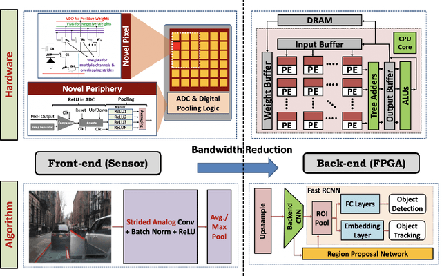
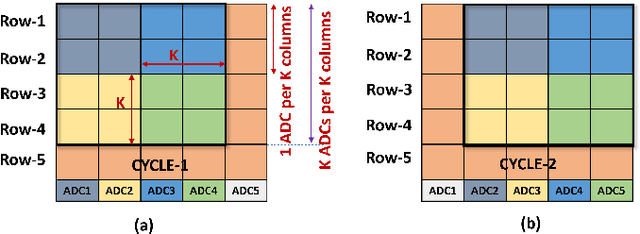
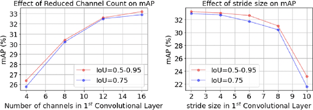
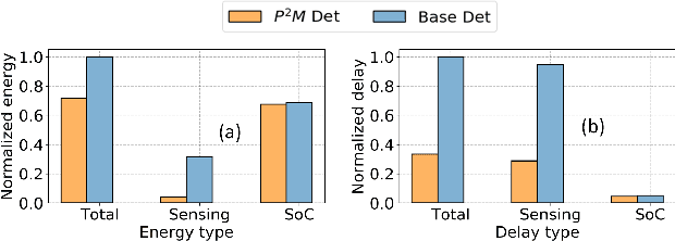
Abstract:Today's high resolution, high frame rate cameras in autonomous vehicles generate a large volume of data that needs to be transferred and processed by a downstream processor or machine learning (ML) accelerator to enable intelligent computing tasks, such as multi-object detection and tracking. The massive amount of data transfer incurs significant energy, latency, and bandwidth bottlenecks, which hinders real-time processing. To mitigate this problem, we propose an algorithm-hardware co-design framework called Processing-in-Pixel-in-Memory-based object Detection and Tracking (P2M-DeTrack). P2M-DeTrack is based on a custom faster R-CNN-based model that is distributed partly inside the pixel array (front-end) and partly in a separate FPGA/ASIC (back-end). The proposed front-end in-pixel processing down-samples the input feature maps significantly with judiciously optimized strided convolution and pooling. Compared to a conventional baseline design that transfers frames of RGB pixels to the back-end, the resulting P2M-DeTrack designs reduce the data bandwidth between sensor and back-end by up to 24x. The designs also reduce the sensor and total energy (obtained from in-house circuit simulations at Globalfoundries 22nm technology node) per frame by 5.7x and 1.14x, respectively. Lastly, they reduce the sensing and total frame latency by an estimated 1.7x and 3x, respectively. We evaluate our approach on the multi-object object detection (tracking) task of the large-scale BDD100K dataset and observe only a 0.5% reduction in the mean average precision (0.8% reduction in the identification F1 score) compared to the state-of-the-art.
P2M: A Processing-in-Pixel-in-Memory Paradigm for Resource-Constrained TinyML Applications
Mar 17, 2022
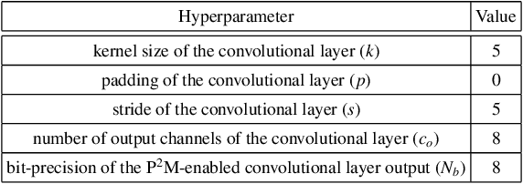
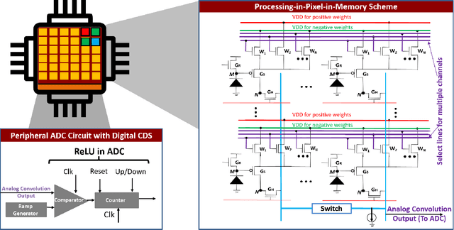

Abstract:The demand to process vast amounts of data generated from state-of-the-art high resolution cameras has motivated novel energy-efficient on-device AI solutions. Visual data in such cameras are usually captured in the form of analog voltages by a sensor pixel array, and then converted to the digital domain for subsequent AI processing using analog-to-digital converters (ADC). Recent research has tried to take advantage of massively parallel low-power analog/digital computing in the form of near- and in-sensor processing, in which the AI computation is performed partly in the periphery of the pixel array and partly in a separate on-board CPU/accelerator. Unfortunately, high-resolution input images still need to be streamed between the camera and the AI processing unit, frame by frame, causing energy, bandwidth, and security bottlenecks. To mitigate this problem, we propose a novel Processing-in-Pixel-in-memory (P2M) paradigm, that customizes the pixel array by adding support for analog multi-channel, multi-bit convolution, batch normalization, and ReLU (Rectified Linear Units). Our solution includes a holistic algorithm-circuit co-design approach and the resulting P2M paradigm can be used as a drop-in replacement for embedding memory-intensive first few layers of convolutional neural network (CNN) models within foundry-manufacturable CMOS image sensor platforms. Our experimental results indicate that P2M reduces data transfer bandwidth from sensors and analog to digital conversions by ~21x, and the energy-delay product (EDP) incurred in processing a MobileNetV2 model on a TinyML use case for visual wake words dataset (VWW) by up to ~11x compared to standard near-processing or in-sensor implementations, without any significant drop in test accuracy.
 Add to Chrome
 Add to Firefox
 Add to Edge