Ajey Jacob
IRIS: Integrated Retinal Functionality in Image Sensors
Aug 14, 2022Abstract:Neuromorphic image sensors draw inspiration from the biological retina to implement visual computations in electronic hardware. Gain control in phototransduction and temporal differentiation at the first retinal synapse inspired the first generation of neuromorphic sensors, but processing in downstream retinal circuits, much of which has been discovered in the past decade, has not been implemented in image sensor technology. We present a technology-circuit co-design solution that implements two motion computations occurring at the output of the retina that could have wide applications for vision based decision making in dynamic environments. Our simulations on Globalfoundries 22nm technology node show that, by taking advantage of the recent advances in semiconductor chip stacking technology, the proposed retina-inspired circuits can be fabricated on image sensing platforms in existing semiconductor foundries. Integrated Retinal Functionality in Image Sensors (IRIS) technology could drive advances in machine vision applications that demand robust, high-speed, energy-efficient and low-bandwidth real-time decision making.
P2M: A Processing-in-Pixel-in-Memory Paradigm for Resource-Constrained TinyML Applications
Mar 17, 2022
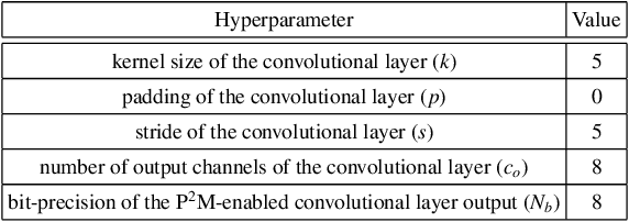
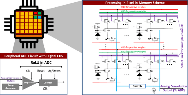

Abstract:The demand to process vast amounts of data generated from state-of-the-art high resolution cameras has motivated novel energy-efficient on-device AI solutions. Visual data in such cameras are usually captured in the form of analog voltages by a sensor pixel array, and then converted to the digital domain for subsequent AI processing using analog-to-digital converters (ADC). Recent research has tried to take advantage of massively parallel low-power analog/digital computing in the form of near- and in-sensor processing, in which the AI computation is performed partly in the periphery of the pixel array and partly in a separate on-board CPU/accelerator. Unfortunately, high-resolution input images still need to be streamed between the camera and the AI processing unit, frame by frame, causing energy, bandwidth, and security bottlenecks. To mitigate this problem, we propose a novel Processing-in-Pixel-in-memory (P2M) paradigm, that customizes the pixel array by adding support for analog multi-channel, multi-bit convolution, batch normalization, and ReLU (Rectified Linear Units). Our solution includes a holistic algorithm-circuit co-design approach and the resulting P2M paradigm can be used as a drop-in replacement for embedding memory-intensive first few layers of convolutional neural network (CNN) models within foundry-manufacturable CMOS image sensor platforms. Our experimental results indicate that P2M reduces data transfer bandwidth from sensors and analog to digital conversions by ~21x, and the energy-delay product (EDP) incurred in processing a MobileNetV2 model on a TinyML use case for visual wake words dataset (VWW) by up to ~11x compared to standard near-processing or in-sensor implementations, without any significant drop in test accuracy.
Toward Efficient Hyperspectral Image Processing inside Camera Pixels
Mar 11, 2022

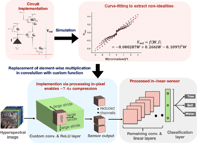

Abstract:Hyperspectral cameras generate a large amount of data due to the presence of hundreds of spectral bands as opposed to only three channels (red, green, and blue) in traditional cameras. This requires a significant amount of data transmission between the hyperspectral image sensor and a processor used to classify/detect/track the images, frame by frame, expending high energy and causing bandwidth and security bottlenecks. To mitigate this problem, we propose a form of processing-in-pixel (PIP) that leverages advanced CMOS technologies to enable the pixel array to perform a wide range of complex operations required by the modern convolutional neural networks (CNN) for hyperspectral image recognition (HSI). Consequently, our PIP-optimized custom CNN layers effectively compress the input data, significantly reducing the bandwidth required to transmit the data downstream to the HSI processing unit. This reduces the average energy consumption associated with pixel array of cameras and the CNN processing unit by 25.06x and 3.90x respectively, compared to existing hardware implementations. Our custom models yield average test accuracies within 0.56% of the baseline models for the standard HSI benchmarks.
Intrinsic Spike Timing Dependent Plasticity in Stochastic Magnetic Tunnel Junctions Mediated by Heat Dynamics
Aug 28, 2021
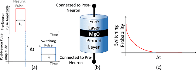

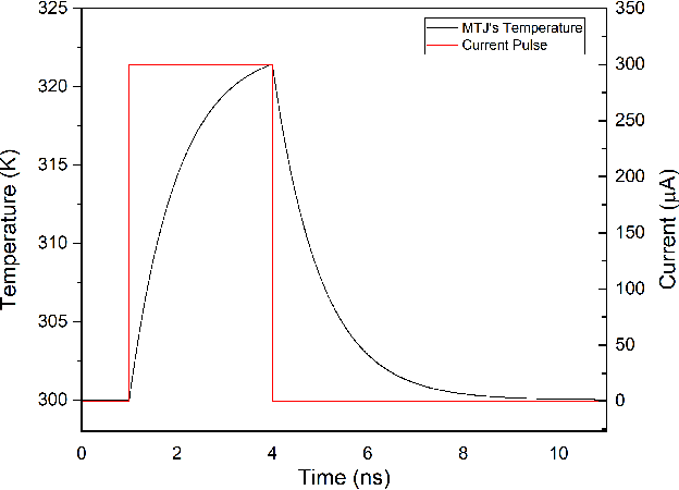
Abstract:The quest for highly efficient cognitive computing has led to extensive research interest for the field of neuromorphic computing. Neuromorphic computing aims to mimic the behavior of biological neurons and synapses using solid-state devices and circuits. Among various approaches, emerging non-volatile memory technologies are of special interest for mimicking neuro-synaptic behavior. These devices allow the mapping of the rich dynamics of biological neurons and synapses onto their intrinsic device physics. In this letter, we focus on Spike Timing Dependent Plasticity (STDP) behavior of biological synapses and propose a method to implement the STDP behavior in Magnetic Tunnel Junction (MTJ) devices. Specifically, we exploit the time-dependent heat dynamics and the response of an MTJ to the instantaneous temperature to imitate the STDP behavior. Our simulations, based on a macro-spin model for magnetization dynamics, show that, STDP can be imitated in stochastic magnetic tunnel junctions by applying simple voltage waveforms as the spiking response of pre- and post-neurons across an MTJ device.
 Add to Chrome
 Add to Firefox
 Add to Edge