John Paul Strachan
Peter Grünberg Institut, RWTH Aachen University
QS4D: Quantization-aware training for efficient hardware deployment of structured state-space sequential models
Jul 08, 2025Abstract:Structured State Space models (SSM) have recently emerged as a new class of deep learning models, particularly well-suited for processing long sequences. Their constant memory footprint, in contrast to the linearly scaling memory demands of Transformers, makes them attractive candidates for deployment on resource-constrained edge-computing devices. While recent works have explored the effect of quantization-aware training (QAT) on SSMs, they typically do not address its implications for specialized edge hardware, for example, analog in-memory computing (AIMC) chips. In this work, we demonstrate that QAT can significantly reduce the complexity of SSMs by up to two orders of magnitude across various performance metrics. We analyze the relation between model size and numerical precision, and show that QAT enhances robustness to analog noise and enables structural pruning. Finally, we integrate these techniques to deploy SSMs on a memristive analog in-memory computing substrate and highlight the resulting benefits in terms of computational efficiency.
Analog In-Memory Computing Attention Mechanism for Fast and Energy-Efficient Large Language Models
Sep 28, 2024


Abstract:Transformer neural networks, driven by self-attention mechanisms, are core components of foundational and Large Language Models. In generative transformers, self-attention uses cache memory to store token projections, avoiding recomputation at each time step. However, GPU-stored projections must be loaded into SRAM for each new generation step, causing latency and energy bottlenecks for long sequences. In this work, we propose a fast and energy-efficient hardware implementation of self-attention using analog in-memory computing based on gain cell memories. Volatile gain cell memories can be efficiently written to store new tokens during sequence generation, while performing analog signed weight multiplications to compute the dot-products required for self-attention. We implement Sliding Window Attention, which keeps memory of a finite set of past steps. A charge-to-pulse converter for array readout eliminates the need for analog-to-digital conversion between self-attention stages. Using a co-designed initialization algorithm to adapt pre-trained weights to gain cell non-idealities, we achieve NLP performance comparable to ChatGPT-2 with minimal training iterations, despite hardware constraints. Our end-to-end hardware design includes digital controls, estimating area, latency, and energy. The system reduces attention latency by up to two orders of magnitude and energy consumption by up to five orders compared to GPUs, marking a significant step toward ultra-fast, low-power sequence generation in Large Language Models.
Roadmap to Neuromorphic Computing with Emerging Technologies
Jul 02, 2024


Abstract:The roadmap is organized into several thematic sections, outlining current computing challenges, discussing the neuromorphic computing approach, analyzing mature and currently utilized technologies, providing an overview of emerging technologies, addressing material challenges, exploring novel computing concepts, and finally examining the maturity level of emerging technologies while determining the next essential steps for their advancement.
Analog Feedback-Controlled Memristor programming Circuit for analog Content Addressable Memory
Apr 21, 2023Abstract:Recent breakthroughs in associative memories suggest that silicon memories are coming closer to human memories, especially for memristive Content Addressable Memories (CAMs) which are capable to read and write in analog values. However, the Program-Verify algorithm, the state-of-the-art memristor programming algorithm, requires frequent switching between verifying and programming memristor conductance, which brings many defects such as high dynamic power and long programming time. Here, we propose an analog feedback-controlled memristor programming circuit that makes use of a novel look-up table-based (LUT-based) programming algorithm. With the proposed algorithm, the programming and the verification of a memristor can be performed in a single-direction sequential process. Besides, we also integrated a single proposed programming circuit with eight analog CAM (aCAM) cells to build an aCAM array. We present SPICE simulations on TSMC 28nm process. The theoretical analysis shows that 1. A memristor conductance within an aCAM cell can be converted to an output boundary voltage in aCAM searching operations and 2. An output boundary voltage in aCAM searching operations can be converted to a programming data line voltage in aCAM programming operations. The simulation results of the proposed programming circuit prove the theoretical analysis and thus verify the feasibility to program memristors without frequently switching between verifying and programming the conductance. Besides, the simulation results of the proposed aCAM array show that the proposed programming circuit can be integrated into a large array architecture.
High-Speed and Energy-Efficient Non-Volatile Silicon Photonic Memory Based on Heterogeneously Integrated Memresonator
Mar 10, 2023Abstract:Recently, interest in programmable photonics integrated circuits has grown as a potential hardware framework for deep neural networks, quantum computing, and field programmable arrays (FPGAs). However, these circuits are constrained by the limited tuning speed and large power consumption of the phase shifters used. In this paper, introduced for the first time are memresonators, or memristors heterogeneously integrated with silicon photonic microring resonators, as phase shifters with non-volatile memory. These devices are capable of retention times of 12 hours, switching voltages lower than 5 V, an endurance of 1,000 switching cycles. Also, these memresonators have been switched using voltage pulses as short as 300 ps with a record low switching energy of 0.15 pJ. Furthermore, these memresonators are fabricated on a heterogeneous III-V/Si platform capable of integrating a rich family of active, passive, and non-linear optoelectronic devices, such as lasers and detectors, directly on-chip to enable in-memory photonic computing and further advance the scalability of integrated photonic processor circuits.
Experimentally realized memristive memory augmented neural network
Apr 15, 2022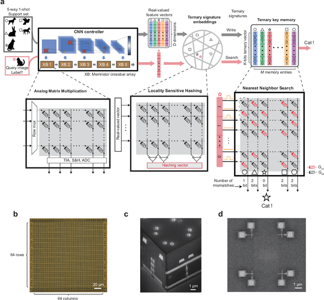
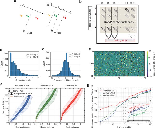
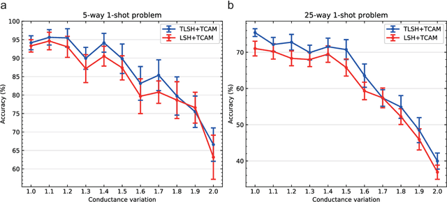
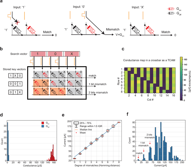
Abstract:Lifelong on-device learning is a key challenge for machine intelligence, and this requires learning from few, often single, samples. Memory augmented neural network has been proposed to achieve the goal, but the memory module has to be stored in an off-chip memory due to its size. Therefore the practical use has been heavily limited. Previous works on emerging memory-based implementation have difficulties in scaling up because different modules with various structures are difficult to integrate on the same chip and the small sense margin of the content addressable memory for the memory module heavily limited the degree of mismatch calculation. In this work, we implement the entire memory augmented neural network architecture in a fully integrated memristive crossbar platform and achieve an accuracy that closely matches standard software on digital hardware for the Omniglot dataset. The successful demonstration is supported by implementing new functions in crossbars in addition to widely reported matrix multiplications. For example, the locality-sensitive hashing operation is implemented in crossbar arrays by exploiting the intrinsic stochasticity of memristor devices. Besides, the content-addressable memory module is realized in crossbars, which also supports the degree of mismatches. Simulations based on experimentally validated models show such an implementation can be efficiently scaled up for one-shot learning on the Mini-ImageNet dataset. The successful demonstration paves the way for practical on-device lifelong learning and opens possibilities for novel attention-based algorithms not possible in conventional hardware.
Prospects for Analog Circuits in Deep Networks
Jun 23, 2021

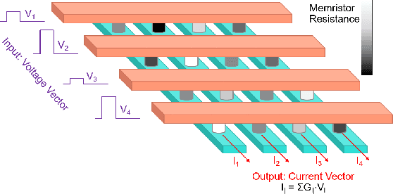

Abstract:Operations typically used in machine learning al-gorithms (e.g. adds and soft max) can be implemented bycompact analog circuits. Analog Application-Specific Integrated Circuit (ASIC) designs that implement these algorithms using techniques such as charge sharing circuits and subthreshold transistors, achieve very high power efficiencies. With the recent advances in deep learning algorithms, focus has shifted to hardware digital accelerator designs that implement the prevalent matrix-vector multiplication operations. Power in these designs is usually dominated by the memory access power of off-chip DRAM needed for storing the network weights and activations. Emerging dense non-volatile memory technologies can help to provide on-chip memory and analog circuits can be well suited to implement the needed multiplication-vector operations coupled with in-computing memory approaches. This paper presents abrief review of analog designs that implement various machine learning algorithms. It then presents an outlook for the use ofanalog circuits in low-power deep network accelerators suitable for edge or tiny machine learning applications.
 Add to Chrome
 Add to Firefox
 Add to Edge