Shao-Yun Fang
LithoHoD: A Litho Simulator-Powered Framework for IC Layout Hotspot Detection
Sep 16, 2024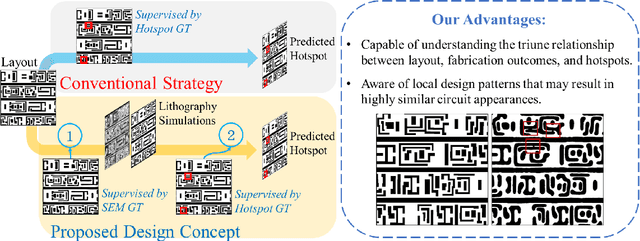
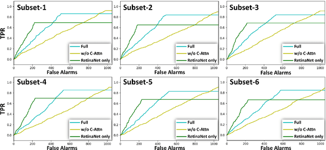
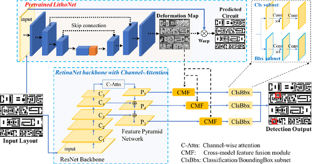
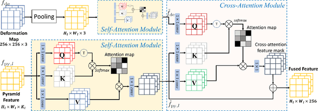
Abstract:Recent advances in VLSI fabrication technology have led to die shrinkage and increased layout density, creating an urgent demand for advanced hotspot detection techniques. However, by taking an object detection network as the backbone, recent learning-based hotspot detectors learn to recognize only the problematic layout patterns in the training data. This fact makes these hotspot detectors difficult to generalize to real-world scenarios. We propose a novel lithography simulator-powered hotspot detection framework to overcome this difficulty. Our framework integrates a lithography simulator with an object detection backbone, merging the extracted latent features from both the simulator and the object detector via well-designed cross-attention blocks. Consequently, the proposed framework can be used to detect potential hotspot regions based on I) the variation of possible circuit shape deformation estimated by the lithography simulator, and ii) the problematic layout patterns already known. To this end, we utilize RetinaNet with a feature pyramid network as the object detection backbone and leverage LithoNet as the lithography simulator. Extensive experiments demonstrate that our proposed simulator-guided hotspot detection framework outperforms previous state-of-the-art methods on real-world data.
Keeping Deep Lithography Simulators Updated: Global-Local Shape-Based Novelty Detection and Active Learning
Jan 24, 2022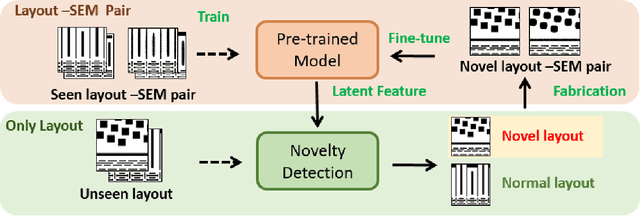
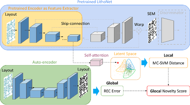
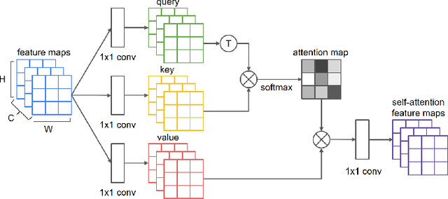

Abstract:Learning-based pre-simulation (i.e., layout-to-fabrication) models have been proposed to predict the fabrication-induced shape deformation from an IC layout to its fabricated circuit. Such models are usually driven by pairwise learning, involving a training set of layout patterns and their reference shape images after fabrication. However, it is expensive and time-consuming to collect the reference shape images of all layout clips for model training and updating. To address the problem, we propose a deep learning-based layout novelty detection scheme to identify novel (unseen) layout patterns, which cannot be well predicted by a pre-trained pre-simulation model. We devise a global-local novelty scoring mechanism to assess the potential novelty of a layout by exploiting two subnetworks: an autoencoder and a pretrained pre-simulation model. The former characterizes the global structural dissimilarity between a given layout and training samples, whereas the latter extracts a latent code representing the fabrication-induced local deformation. By integrating the global dissimilarity with the local deformation boosted by a self-attention mechanism, our model can accurately detect novelties without the ground-truth circuit shapes of test samples. Based on the detected novelties, we further propose two active-learning strategies to sample a reduced amount of representative layouts most worthy to be fabricated for acquiring their ground-truth circuit shapes. Experimental results demonstrate i) our method's effectiveness in layout novelty detection, and ii) our active-learning strategies' ability in selecting representative novel layouts for keeping a learning-based pre-simulation model updated.
FIST: A Feature-Importance Sampling and Tree-Based Method for Automatic Design Flow Parameter Tuning
Nov 26, 2020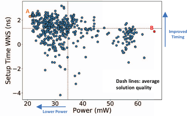
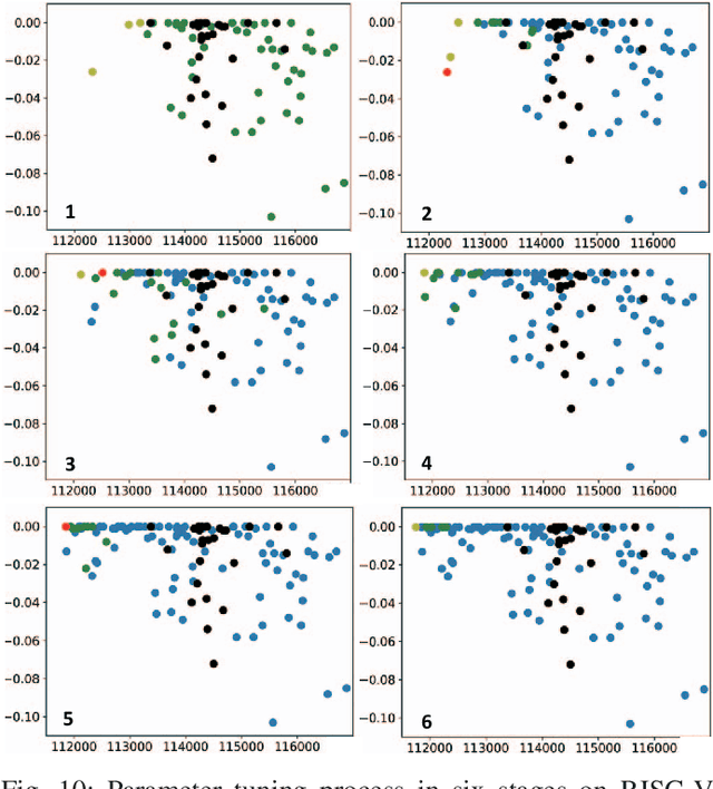
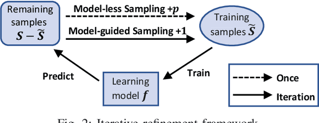
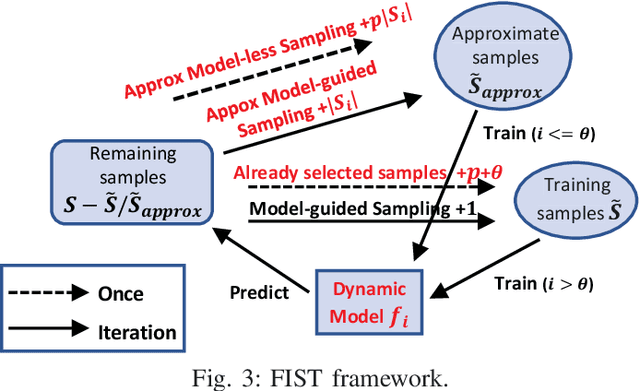
Abstract:Design flow parameters are of utmost importance to chip design quality and require a painfully long time to evaluate their effects. In reality, flow parameter tuning is usually performed manually based on designers' experience in an ad hoc manner. In this work, we introduce a machine learning-based automatic parameter tuning methodology that aims to find the best design quality with a limited number of trials. Instead of merely plugging in machine learning engines, we develop clustering and approximate sampling techniques for improving tuning efficiency. The feature extraction in this method can reuse knowledge from prior designs. Furthermore, we leverage a state-of-the-art XGBoost model and propose a novel dynamic tree technique to overcome overfitting. Experimental results on benchmark circuits show that our approach achieves 25% improvement in design quality or 37% reduction in sampling cost compared to random forest method, which is the kernel of a highly cited previous work. Our approach is further validated on two industrial designs. By sampling less than 0.02% of possible parameter sets, it reduces area by 1.83% and 1.43% compared to the best solutions hand-tuned by experienced designers.
From IC Layout to Die Photo: A CNN-Based Data-Driven Approach
Feb 11, 2020
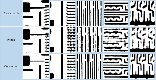
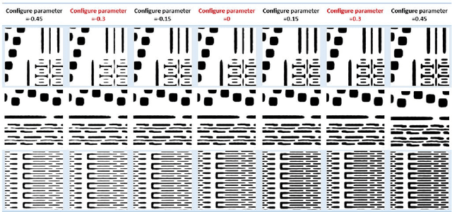
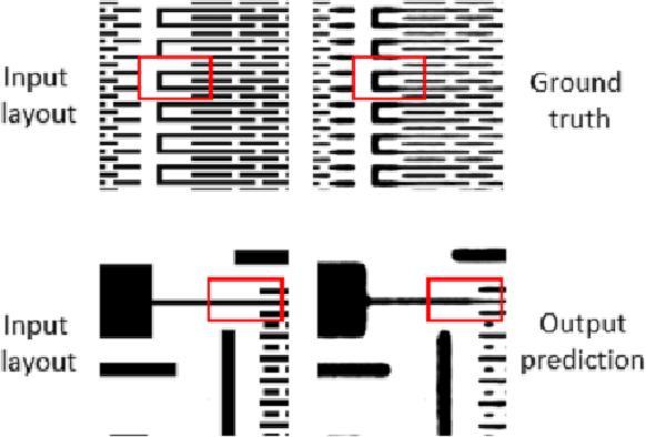
Abstract:Since IC fabrication is costly and time-consuming, it is highly desirable to develop virtual metrology tools that can predict the properties of a wafer based on fabrication configurations without performing physical measurements on a fabricated IC. We propose a deep learning-based data-driven framework consisting of two convolutional neural networks: i) LithoNet that predicts the shape deformations on a circuit due to IC fabrication, and ii) OPCNet that suggests IC layout corrections to compensate for such shape deformations. By learning the shape correspondence between pairs of layout design patterns and their SEM images of the product wafer thereof, given an IC layout pattern, LithoNet can mimic the fabrication procedure to predict its fabricated circuit shape for virtual metrology. Furthermore, LithoNet can take the wafer fabrication parameters as a latent vector to model the parametric product variations that can be inspected on SEM images. In addition, traditional lithography simulation methods used to suggest a correction on a lithographic photomask is computationally expensive. Our proposed OPCNet mimics the optical proximity correction (OPC) procedure and efficiently generates a corrected photomask by collaborating with LithoNet to examine if the shape of a fabricated IC circuitry best matches its original layout design. As a result, the proposed LithoNet-OPCNet framework cannot only predict the shape of a fabricated IC from its layout pattern, but also suggests a layout correction according to the consistency between the predicted shape and the given layout. Experimental results with several benchmark layout patterns demonstrate the effectiveness of the proposed method.
 Add to Chrome
 Add to Firefox
 Add to Edge