From IC Layout to Die Photo: A CNN-Based Data-Driven Approach
Paper and Code
Feb 11, 2020


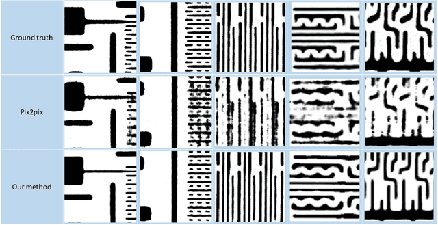
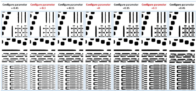
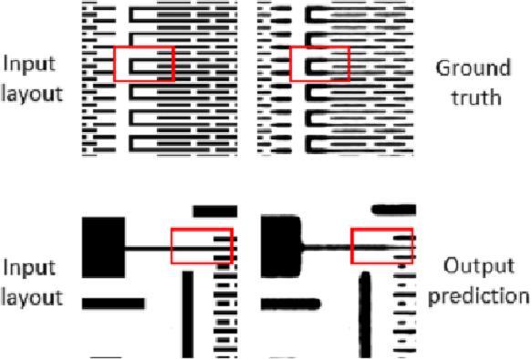
Since IC fabrication is costly and time-consuming, it is highly desirable to develop virtual metrology tools that can predict the properties of a wafer based on fabrication configurations without performing physical measurements on a fabricated IC. We propose a deep learning-based data-driven framework consisting of two convolutional neural networks: i) LithoNet that predicts the shape deformations on a circuit due to IC fabrication, and ii) OPCNet that suggests IC layout corrections to compensate for such shape deformations. By learning the shape correspondence between pairs of layout design patterns and their SEM images of the product wafer thereof, given an IC layout pattern, LithoNet can mimic the fabrication procedure to predict its fabricated circuit shape for virtual metrology. Furthermore, LithoNet can take the wafer fabrication parameters as a latent vector to model the parametric product variations that can be inspected on SEM images. In addition, traditional lithography simulation methods used to suggest a correction on a lithographic photomask is computationally expensive. Our proposed OPCNet mimics the optical proximity correction (OPC) procedure and efficiently generates a corrected photomask by collaborating with LithoNet to examine if the shape of a fabricated IC circuitry best matches its original layout design. As a result, the proposed LithoNet-OPCNet framework cannot only predict the shape of a fabricated IC from its layout pattern, but also suggests a layout correction according to the consistency between the predicted shape and the given layout. Experimental results with several benchmark layout patterns demonstrate the effectiveness of the proposed method.
 Add to Chrome
 Add to Firefox
 Add to Edge