 Add to Chrome
 Add to Firefox
 Add to Edge
MAPS: Multi-Fidelity AI-Augmented Photonic Simulation and Inverse Design Infrastructure
Mar 02, 2025


Inverse design has emerged as a transformative approach for photonic device optimization, enabling the exploration of high-dimensional, non-intuitive design spaces to create ultra-compact devices and advance photonic integrated circuits (PICs) in computing and interconnects. However, practical challenges, such as suboptimal device performance, limited manufacturability, high sensitivity to variations, computational inefficiency, and lack of interpretability, have hindered its adoption in commercial hardware. Recent advancements in AI-assisted photonic simulation and design offer transformative potential, accelerating simulations and design generation by orders of magnitude over traditional numerical methods. Despite these breakthroughs, the lack of an open-source, standardized infrastructure and evaluation benchmark limits accessibility and cross-disciplinary collaboration. To address this, we introduce MAPS, a multi-fidelity AI-augmented photonic simulation and inverse design infrastructure designed to bridge this gap. MAPS features three synergistic components: (1) MAPS-Data: A dataset acquisition framework for generating multi-fidelity, richly labeled devices, providing high-quality data for AI-for-optics research. (2) MAPS-Train: A flexible AI-for-photonics training framework offering a hierarchical data loading pipeline, customizable model construction, support for data- and physics-driven losses, and comprehensive evaluations. (3) MAPS-InvDes: An advanced adjoint inverse design toolkit that abstracts complex physics but exposes flexible optimization steps, integrates pre-trained AI models, and incorporates fabrication variation models. This infrastructure MAPS provides a unified, open-source platform for developing, benchmarking, and advancing AI-assisted photonic design workflows, accelerating innovation in photonic hardware optimization and scientific machine learning.
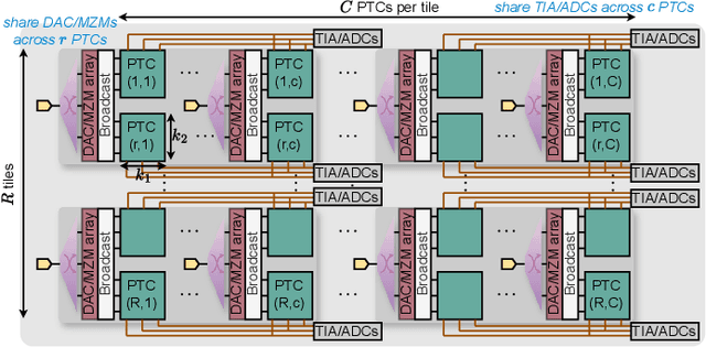
SimPhony: A Device-Circuit-Architecture Cross-Layer Modeling and Simulation Framework for Heterogeneous Electronic-Photonic AI System
Nov 20, 2024


Electronic-photonic integrated circuits (EPICs) offer transformative potential for next-generation high-performance AI but require interdisciplinary advances across devices, circuits, architecture, and design automation. The complexity of hybrid systems makes it challenging even for domain experts to understand distinct behaviors and interactions across design stack. The lack of a flexible, accurate, fast, and easy-to-use EPIC AI system simulation framework significantly limits the exploration of hardware innovations and system evaluations on common benchmarks. To address this gap, we propose SimPhony, a cross-layer modeling and simulation framework for heterogeneous electronic-photonic AI systems. SimPhony offers a platform that enables (1) generic, extensible hardware topology representation that supports heterogeneous multi-core architectures with diverse photonic tensor core designs; (2) optics-specific dataflow modeling with unique multi-dimensional parallelism and reuse beyond spatial/temporal dimensions; (3) data-aware energy modeling with realistic device responses, layout-aware area estimation, link budget analysis, and bandwidth-adaptive memory modeling; and (4) seamless integration with model training framework for hardware/software co-simulation. By providing a unified, versatile, and high-fidelity simulation platform, SimPhony enables researchers to innovate and evaluate EPIC AI hardware across multiple domains, facilitating the next leap in emerging AI hardware. We open-source our codes at https://github.com/ScopeX-ASU/SimPhony
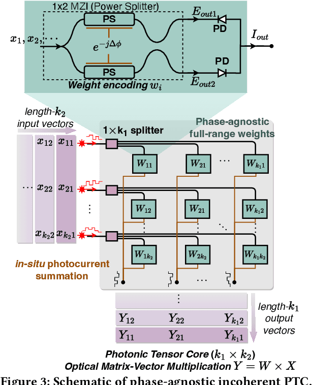
ADEPT-Z: Zero-Shot Automated Circuit Topology Search for Pareto-Optimal Photonic Tensor Cores
Oct 02, 2024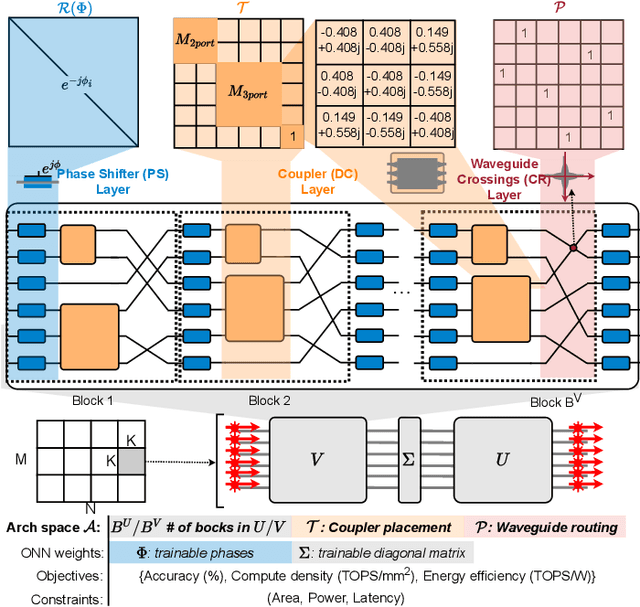
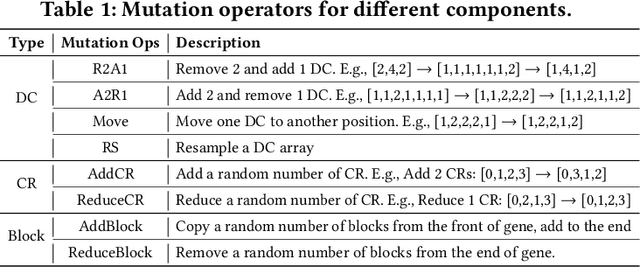
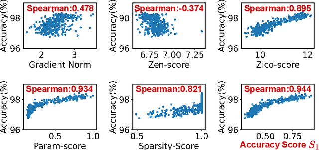

Photonic tensor cores (PTCs) are essential building blocks for optical artificial intelligence (AI) accelerators based on programmable photonic integrated circuits. Most PTC designs today are manually constructed, with low design efficiency and unsatisfying solution quality. This makes it challenging to meet various hardware specifications and keep up with rapidly evolving AI applications. Prior work has explored gradient-based methods to learn a good PTC structure differentiably. However, it suffers from slow training speed and optimization difficulty when handling multiple non-differentiable objectives and constraints. Therefore, in this work, we propose a more flexible and efficient zero-shot multi-objective evolutionary topology search framework ADEPT-Z that explores Pareto-optimal PTC designs with advanced devices in a larger search space. Multiple objectives can be co-optimized while honoring complicated hardware constraints. With only <3 hours of search, we can obtain tens of diverse Pareto-optimal solutions, 100x faster than the prior gradient-based method, outperforming prior manual designs with 2x higher accuracy weighted area-energy efficiency. The code of ADEPT-Z is available at https://github.com/ScopeX-ASU/ADEPT-Z.
SCATTER: Algorithm-Circuit Co-Sparse Photonic Accelerator with Thermal-Tolerant, Power-Efficient In-situ Light Redistribution
Jul 07, 2024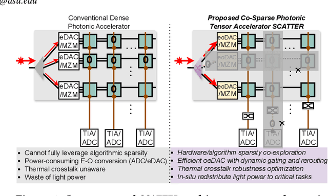
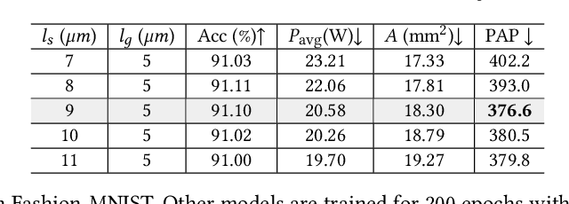
Photonic computing has emerged as a promising solution for accelerating computation-intensive artificial intelligence (AI) workloads. However, limited reconfigurability, high electrical-optical conversion cost, and thermal sensitivity limit the deployment of current optical analog computing engines to support power-restricted, performance-sensitive AI workloads at scale. Sparsity provides a great opportunity for hardware-efficient AI accelerators. However, current dense photonic accelerators fail to fully exploit the power-saving potential of algorithmic sparsity. It requires sparsity-aware hardware specialization with a fundamental re-design of photonic tensor core topology and cross-layer device-circuit-architecture-algorithm co-optimization aware of hardware non-ideality and power bottleneck. To trim down the redundant power consumption while maximizing robustness to thermal variations, we propose SCATTER, a novel algorithm-circuit co-sparse photonic accelerator featuring dynamically reconfigurable signal path via thermal-tolerant, power-efficient in-situ light redistribution and power gating. A power-optimized, crosstalk-aware dynamic sparse training framework is introduced to explore row-column structured sparsity and ensure marginal accuracy loss and maximum power efficiency. The extensive evaluation shows that our cross-stacked optimized accelerator SCATTER achieves a 511X area reduction and 12.4X power saving with superior crosstalk tolerance that enables unprecedented circuit layout compactness and on-chip power efficiency.