Sudip Shekhar
Dynamic Beam-Stabilized, Additive-Printed Flexible Antenna Arrays with On-Chip Rapid Insight Generation
May 15, 2025Abstract:Conformal phased arrays promise shape-changing properties, multiple degrees of freedom to the scan angle, and novel applications in wearables, aerospace, defense, vehicles, and ships. However, they have suffered from two critical limitations. (1) Although most applications require on-the-move communication and sensing, prior conformal arrays have suffered from dynamic deformation-induced beam pointing errors. We introduce a Dynamic Beam-Stabilized (DBS) processor capable of beam adaptation through on-chip real-time control of fundamental gain, phase, and delay for each element. (2) Prior conformal arrays have leveraged additive printing to enhance flexibility, but conventional printable inks based on silver are expensive, and those based on copper suffer from spontaneous metal oxidation that alters trace impedance and degrades beamforming performance. We instead leverage a low-cost Copper Molecular Decomposition (CuMOD) ink with < 0.1% variation per degree C with temperature and strain and correct any residual deformity in real-time using the DBS processor. Demonstrating unified material and physical deformation correction, our CMOS DBS processor is low power, low-area, and easily scalable due to a tile architecture, thereby ideal for on-device implementations.
Real-time Deformation Correction in Additively Printed Flexible Antenna Arrays
Jun 12, 2024Abstract:Conformal phased arrays provide multiple degrees of freedom to the scan angle, which is typically limited by antenna aperture in rigid arrays. Silicon-based RF signal processing offers reliable, reconfigurable, multi-functional, and compact control for conformal phased arrays that can be used for on-the-move communication. While the lightweight, compactness, and shape-changing properties of the conformal phased arrays are attractive, these features result in dynamic deformation of the array during motion leading to significant dynamic beam pointing errors. We propose a silicon-based, compact, reconfigurable solution to self-correct these dynamic deformation-induced beam pointing errors. Furthermore, additive printing is leveraged to enhance the flexibility of the conformal phased arrays, as the printed conductive ink is more flexible than bulk copper and can be easily deposited on flexible sheets using different printing tools, providing an environmentally-friendly solution for large-scale production. The inks such as conventional silver inks are expensive and copper-based printable inks suffer from spontaneous metal oxidation that alters trace impedance and degrades beamforming performance. This work uses a low-cost molecular copper decomposition ink with reliable RF properties at different temperature and strain to print the proposed intelligent conformal phased array operating at 2.1 GHz. Proof-of-concept prototype $2\times2$ array self-corrects the deformation induces beampointing error with an error $<1.25^\circ$. The silicon based array processing part occupying only 2.56 mm$^2$ area and 78.5 mW power per tile.
Dynamic Electro-Optic Analog Memory for Neuromorphic Photonic Computing
Jan 29, 2024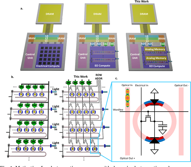

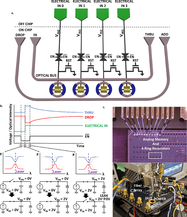
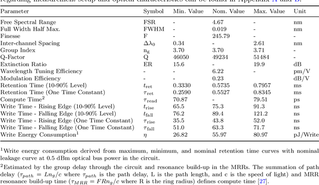
Abstract:Artificial intelligence (AI) has seen remarkable advancements across various domains, including natural language processing, computer vision, autonomous vehicles, and biology. However, the rapid expansion of AI technologies has escalated the demand for more powerful computing resources. As digital computing approaches fundamental limits, neuromorphic photonics emerges as a promising platform to complement existing digital systems. In neuromorphic photonic computing, photonic devices are controlled using analog signals. This necessitates the use of digital-to-analog converters (DAC) and analog-to-digital converters (ADC) for interfacing with these devices during inference and training. However, data movement between memory and these converters in conventional von Neumann computing architectures consumes energy. To address this, analog memory co-located with photonic computing devices is proposed. This approach aims to reduce the reliance on DACs and ADCs and minimize data movement to enhance compute efficiency. This paper demonstrates a monolithically integrated neuromorphic photonic circuit with co-located capacitive analog memory and compares various analog memory technologies for neuromorphic photonic computing using the MNIST dataset as a benchmark.
Monolithic Silicon Photonic Architecture for Training Deep Neural Networks with Direct Feedback Alignment
Nov 12, 2021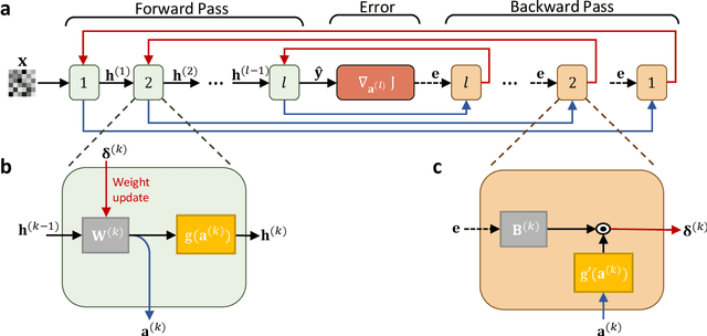
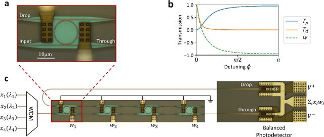
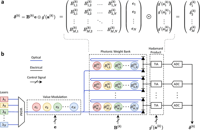

Abstract:The field of artificial intelligence (AI) has witnessed tremendous growth in recent years, however some of the most pressing challenges for the continued development of AI systems are the fundamental bandwidth, energy efficiency, and speed limitations faced by electronic computer architectures. There has been growing interest in using photonic processors for performing neural network inference operations, however these networks are currently trained using standard digital electronics. Here, we propose on-chip training of neural networks enabled by a CMOS-compatible silicon photonic architecture to harness the potential for massively parallel, efficient, and fast data operations. Our scheme employs the direct feedback alignment training algorithm, which trains neural networks using error feedback rather than error backpropagation, and can operate at speeds of trillions of multiply-accumulate (MAC) operations per second while consuming less than one picojoule per MAC operation. The photonic architecture exploits parallelized matrix-vector multiplications using arrays of microring resonators for processing multi-channel analog signals along single waveguide buses to calculate the gradient vector of each neural network layer in situ, which is the most computationally expensive operation performed during the backward pass. We also experimentally demonstrate training a deep neural network with the MNIST dataset using on-chip MAC operation results. Our novel approach for efficient, ultra-fast neural network training showcases photonics as a promising platform for executing AI applications.
 Add to Chrome
 Add to Firefox
 Add to Edge