Lukas Chrostowski
Dynamic Electro-Optic Analog Memory for Neuromorphic Photonic Computing
Jan 29, 2024


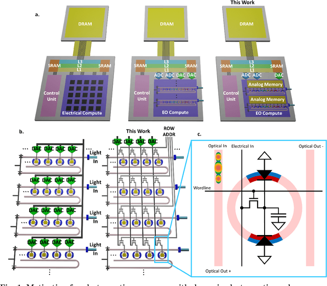
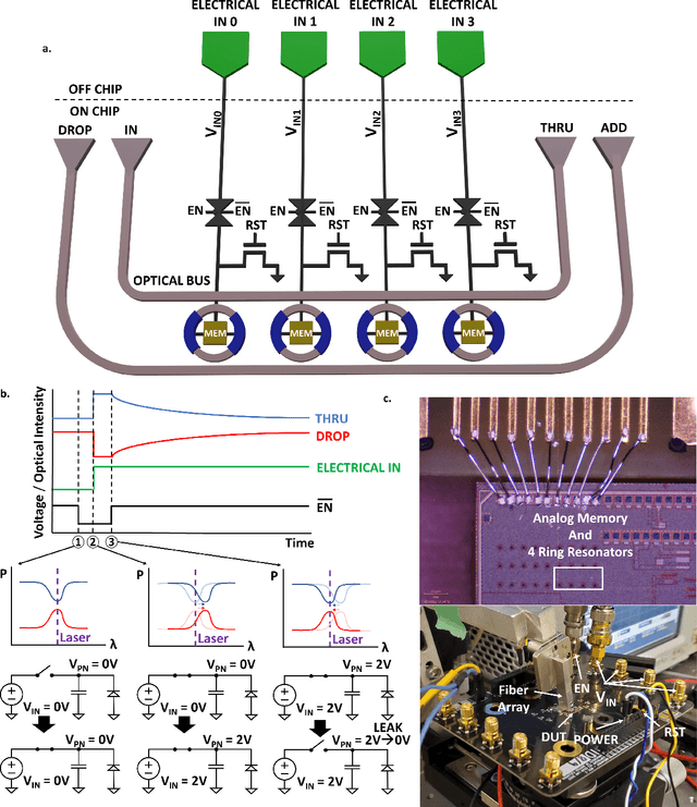
Abstract:Artificial intelligence (AI) has seen remarkable advancements across various domains, including natural language processing, computer vision, autonomous vehicles, and biology. However, the rapid expansion of AI technologies has escalated the demand for more powerful computing resources. As digital computing approaches fundamental limits, neuromorphic photonics emerges as a promising platform to complement existing digital systems. In neuromorphic photonic computing, photonic devices are controlled using analog signals. This necessitates the use of digital-to-analog converters (DAC) and analog-to-digital converters (ADC) for interfacing with these devices during inference and training. However, data movement between memory and these converters in conventional von Neumann computing architectures consumes energy. To address this, analog memory co-located with photonic computing devices is proposed. This approach aims to reduce the reliance on DACs and ADCs and minimize data movement to enhance compute efficiency. This paper demonstrates a monolithically integrated neuromorphic photonic circuit with co-located capacitive analog memory and compares various analog memory technologies for neuromorphic photonic computing using the MNIST dataset as a benchmark.
Reinforcement Learning for Photonic Component Design
Jul 14, 2023Abstract:We present a new fab-in-the-loop reinforcement learning algorithm for the design of nano-photonic components that accounts for the imperfections present in nanofabrication processes. As a demonstration of the potential of this technique, we apply it to the design of photonic crystal grating couplers (PhCGC) fabricated on a 220nm silicon on insulator (SOI) single etch platform. This fab-in-the-loop algorithm improves the insertion loss from 8.8 dB to 3.24 dB. The widest bandwidth designs produced using our fab-in-the-loop algorithm are able to cover a 150nm bandwidth with less than 10.2 dB of loss at their lowest point.
 Add to Chrome
 Add to Firefox
 Add to Edge