Shichen Qiao
ZFusion: An Effective Fuser of Camera and 4D Radar for 3D Object Perception in Autonomous Driving
Apr 07, 2025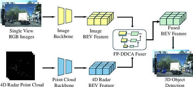

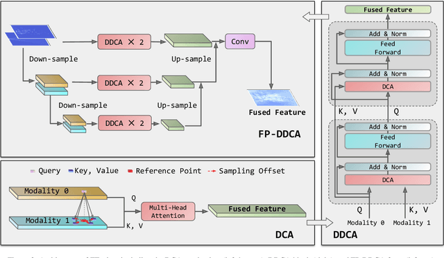

Abstract:Reliable 3D object perception is essential in autonomous driving. Owing to its sensing capabilities in all weather conditions, 4D radar has recently received much attention. However, compared to LiDAR, 4D radar provides much sparser point cloud. In this paper, we propose a 3D object detection method, termed ZFusion, which fuses 4D radar and vision modality. As the core of ZFusion, our proposed FP-DDCA (Feature Pyramid-Double Deformable Cross Attention) fuser complements the (sparse) radar information and (dense) vision information, effectively. Specifically, with a feature-pyramid structure, the FP-DDCA fuser packs Transformer blocks to interactively fuse multi-modal features at different scales, thus enhancing perception accuracy. In addition, we utilize the Depth-Context-Split view transformation module due to the physical properties of 4D radar. Considering that 4D radar has a much lower cost than LiDAR, ZFusion is an attractive alternative to LiDAR-based methods. In typical traffic scenarios like the VoD (View-of-Delft) dataset, experiments show that with reasonable inference speed, ZFusion achieved the state-of-the-art mAP (mean average precision) in the region of interest, while having competitive mAP in the entire area compared to the baseline methods, which demonstrates performance close to LiDAR and greatly outperforms those camera-only methods.
Low-probability of Intercept/Detect (LPI/LPD) Secure Communications Using Antenna Arrays Employing Rapid Sidelobe Time Modulation
Jun 17, 2024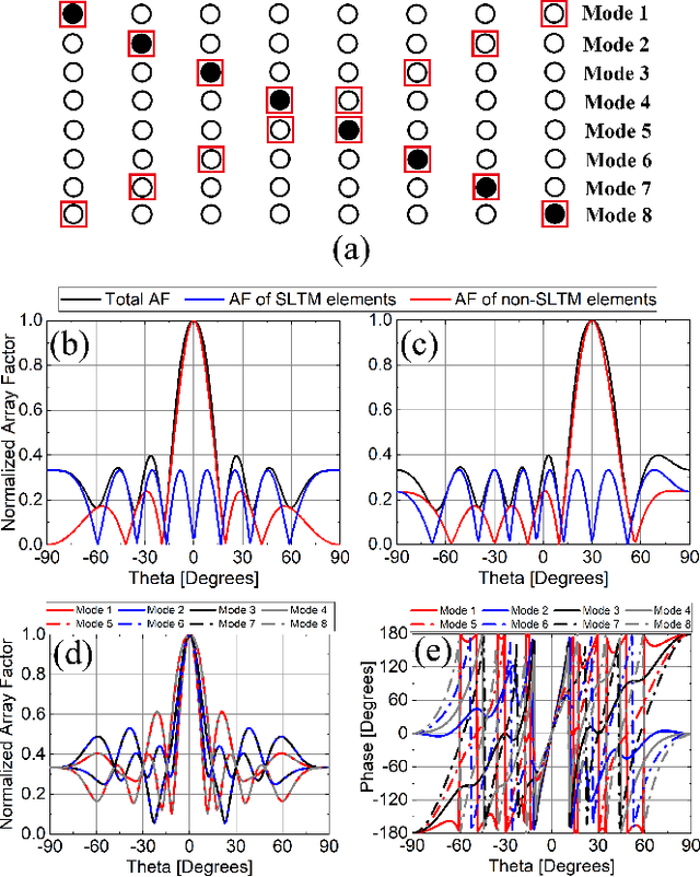


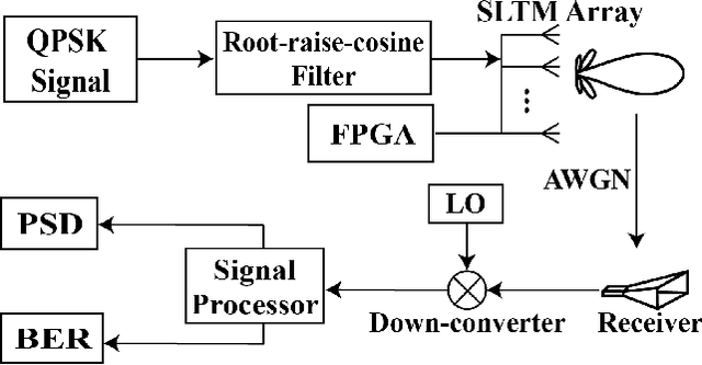
Abstract:We present an electronically-reconfigurable antenna array offering low probability of intercept/detect (LPI/LPD) and secure communications capabilities simultaneously at the physical layer. This antenna array is designed to provide rapidly time-varying sidelobes and a stationary main lobe. By performing rapid sidelobe time modulation (SLTM), the signal transmitted in the undesired directions (i.e., through sidelobes) undergoes spread-spectrum distortion making it more difficult to be detected, intercepted, and deciphered while the signal transmitted in the desired direction (i.e., through the main lobe) is unaffected. Therefore, the intended receiver would not need additional modifications (i.e. encryption keys) to detect and recover the signal. We describe the operating principles of this SLTM array and validate its spread-spectrum SLTM sequence generation in undesired directions through theory, simulations, and experiments. Using a fabricated SLTM prototype operating at X band, we conducted system-level measurements to demonstrate its LPI/LPD, secure communications, and jamming resilience capabilities. The presented method is a physical layer technique, which can bring LPI/LPD capabilities to existing communications systems by simply replacing their antennas with SLTM arrays. This technique can be used independently or in combination with additional coding and signal-processing techniques to achieve further enhancements in LPI/LPD and secure communications.
FPGA Implementation of Convolutional Neural Network for Real-Time Handwriting Recognition
Jun 26, 2023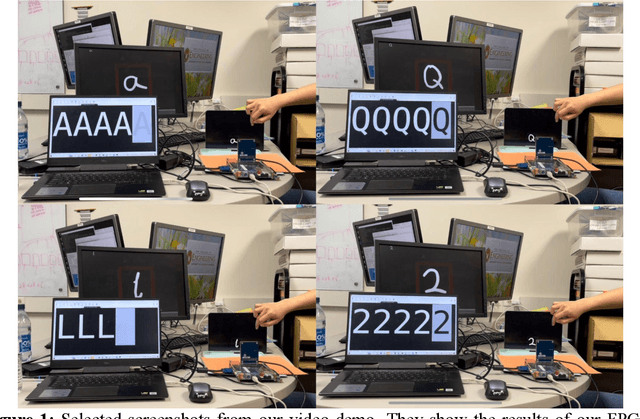
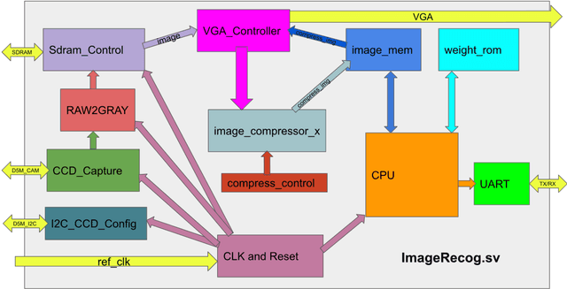
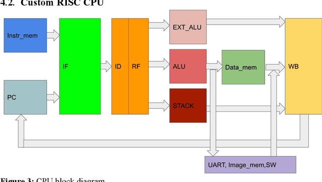
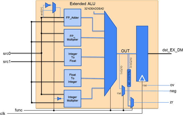
Abstract:Machine Learning (ML) has recently been a skyrocketing field in Computer Science. As computer hardware engineers, we are enthusiastic about hardware implementations of popular software ML architectures to optimize their performance, reliability, and resource usage. In this project, we designed a highly-configurable, real-time device for recognizing handwritten letters and digits using an Altera DE1 FPGA Kit. We followed various engineering standards, including IEEE-754 32-bit Floating-Point Standard, Video Graphics Array (VGA) display protocol, Universal Asynchronous Receiver-Transmitter (UART) protocol, and Inter-Integrated Circuit (I2C) protocols to achieve the project goals. These significantly improved our design in compatibility, reusability, and simplicity in verifications. Following these standards, we designed a 32-bit floating-point (FP) instruction set architecture (ISA). We developed a 5-stage RISC processor in System Verilog to manage image processing, matrix multiplications, ML classifications, and user interfaces. Three different ML architectures were implemented and evaluated on our design: Linear Classification (LC), a 784-64-10 fully connected neural network (NN), and a LeNet-like Convolutional Neural Network (CNN) with ReLU activation layers and 36 classes (10 for the digits and 26 for the case-insensitive letters). The training processes were done in Python scripts, and the resulting kernels and weights were stored in hex files and loaded into the FPGA's SRAM units. Convolution, pooling, data management, and various other ML features were guided by firmware in our custom assembly language. This paper documents the high-level design block diagrams, interfaces between each System Verilog module, implementation details of our software and firmware components, and further discussions on potential impacts.
 Add to Chrome
 Add to Firefox
 Add to Edge