Eric J. Hoffman
FPGA Implementation of Convolutional Neural Network for Real-Time Handwriting Recognition
Jun 26, 2023


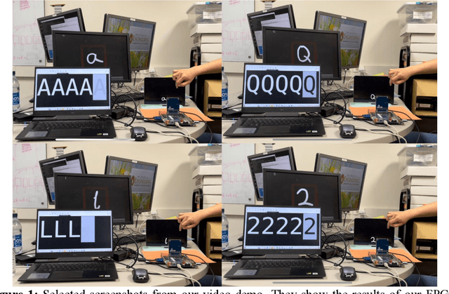
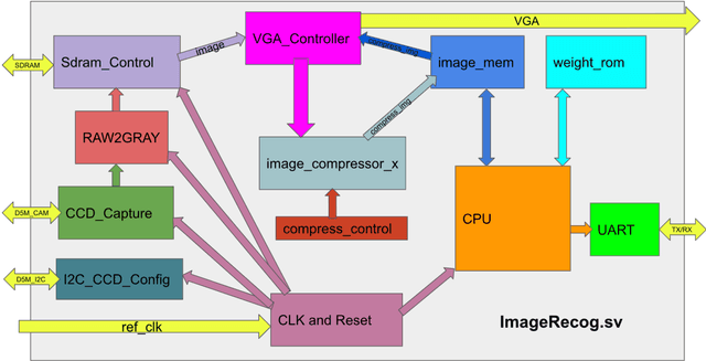
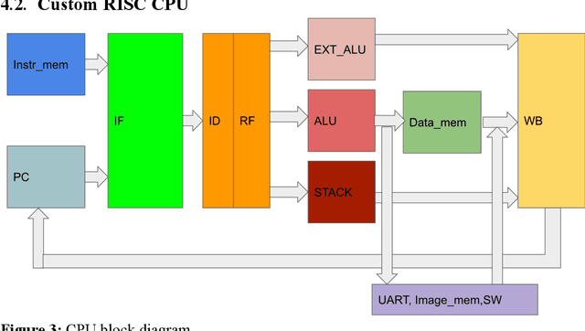
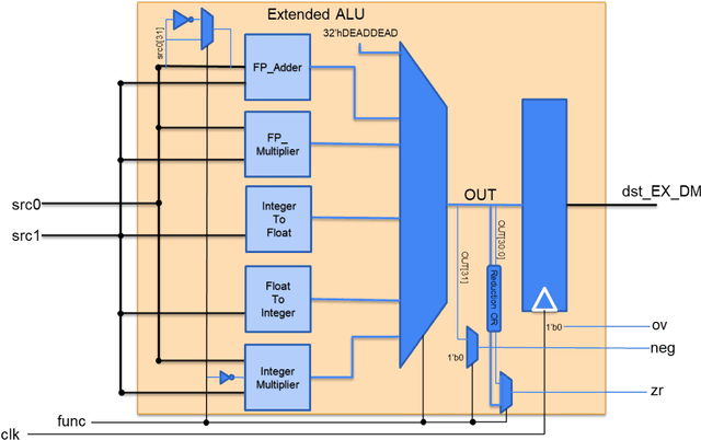
Abstract:Machine Learning (ML) has recently been a skyrocketing field in Computer Science. As computer hardware engineers, we are enthusiastic about hardware implementations of popular software ML architectures to optimize their performance, reliability, and resource usage. In this project, we designed a highly-configurable, real-time device for recognizing handwritten letters and digits using an Altera DE1 FPGA Kit. We followed various engineering standards, including IEEE-754 32-bit Floating-Point Standard, Video Graphics Array (VGA) display protocol, Universal Asynchronous Receiver-Transmitter (UART) protocol, and Inter-Integrated Circuit (I2C) protocols to achieve the project goals. These significantly improved our design in compatibility, reusability, and simplicity in verifications. Following these standards, we designed a 32-bit floating-point (FP) instruction set architecture (ISA). We developed a 5-stage RISC processor in System Verilog to manage image processing, matrix multiplications, ML classifications, and user interfaces. Three different ML architectures were implemented and evaluated on our design: Linear Classification (LC), a 784-64-10 fully connected neural network (NN), and a LeNet-like Convolutional Neural Network (CNN) with ReLU activation layers and 36 classes (10 for the digits and 26 for the case-insensitive letters). The training processes were done in Python scripts, and the resulting kernels and weights were stored in hex files and loaded into the FPGA's SRAM units. Convolution, pooling, data management, and various other ML features were guided by firmware in our custom assembly language. This paper documents the high-level design block diagrams, interfaces between each System Verilog module, implementation details of our software and firmware components, and further discussions on potential impacts.
 Add to Chrome
 Add to Firefox
 Add to Edge