Baibhab Chatterjee
A Systematic Method for Optimum Biomedical Wireless Power Transfer using Inductive Links in Area-Constrained Implants
Jan 15, 2025


Abstract:In the context of implantable bioelectronics, this work provides new insights into maximizing biomedical wireless power transfer (BWPT) via the systematic development of inductive links. This approach addresses the specific challenges of power transfer efficiency (PTE) optimization within the area constraints of bio-implants embedded in tissue. Key contributions include the derivation of an optimal self-inductance with S-parameter-based analyses leading to the co-design of planar spiral coils and L-section impedance matching networks. To validate the proposed design methodology, two coil prototypes -- one symmetric (type-1) and one asymmetric (type-2) -- were fabricated and tested for PTE in pork tissue. Targeting a 20 MHz design frequency, the type-1 coil demonstrated a state-of-the-art PTE of $\sim$ 4\% (channel length = 15 mm) with a return loss (RL) $>$ 20 dB on both the input and output sides, within an area constraint of $<$ 18 $ \times $ 18 mm$^{2}$. In contrast, the type-2 coil achieved a PTE of $\sim$ 2\% with an RL $>$ 15 dB, for a smaller receiving coil area of $<$ 5x5 mm$^{2}$ for the same tissue environment. To complement the coils, we demonstrate a 65 nm test chip with an integrated energy harvester, which includes \asif{a} 30-stage rectifier and low-dropout regulator (LDO), producing a stable $\sim$ 1V DC output within tissue medium, matching theoretical predictions and simulations. Furthermore, we provide a robust and comprehensive guideline for advancing efficient inductive links for various BWPT applications, with shared resources in GitHub available for utilization by the broader community.
Galvanic Body-Coupled Powering for Wireless Implanted Neurostimulators
Dec 04, 2024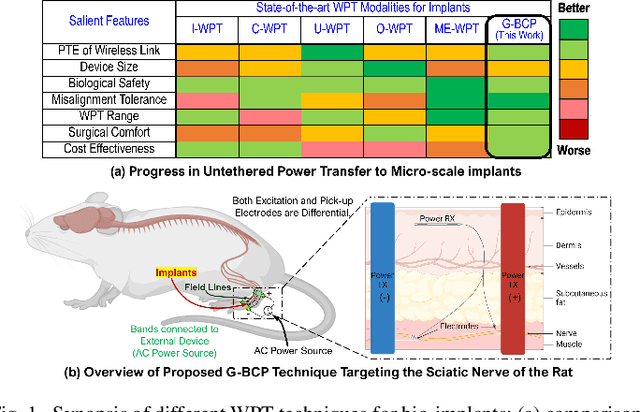
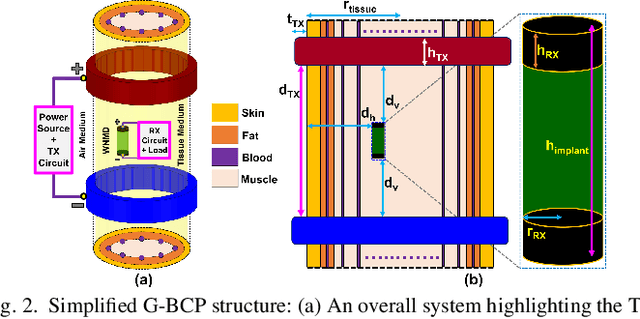
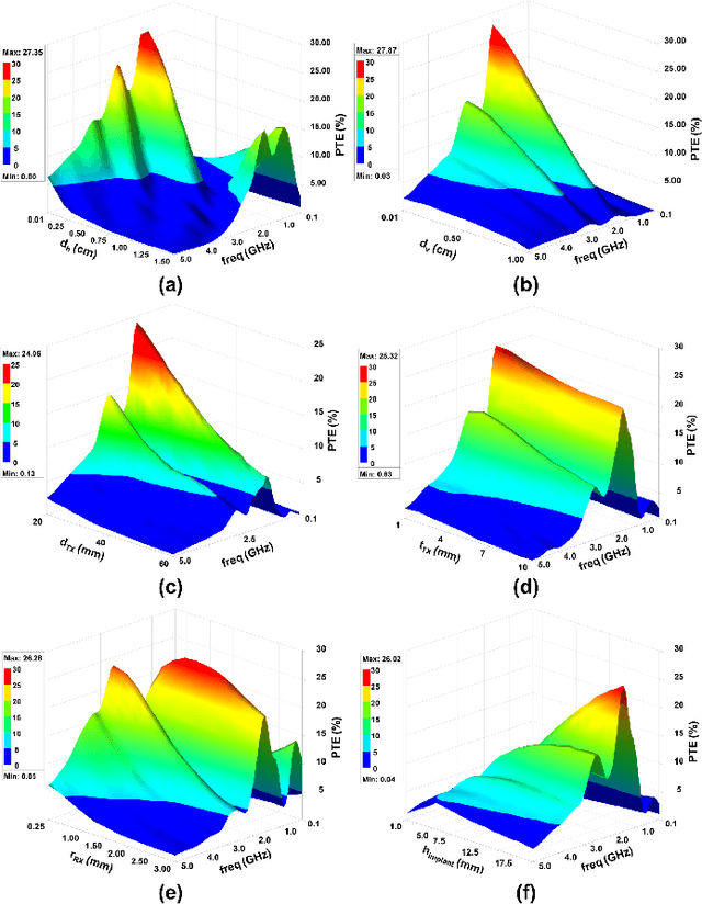
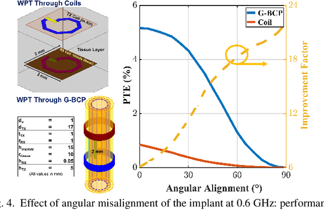
Abstract:Body-coupled powering (BCP) is an innovative wireless power transfer (WPT) technique, recently explored for its potential to deliver power to cutting-edge biomedical implants such as nerve and muscle stimulators. This paper demonstrates the efficient technique of designing WPT systems embedding BCP via galvanic coupling (G-BCP). The G-BCP configuration utilizes two metal circular rings surrounding the body area of interest as the transmitter (TX) electrodes required for galvanic (differential) excitation and a wireless implant as the receiver (RX) equipped with two electrodes for differential power reception accordingly. By focusing on the unique advantages of this approach - such as enhanced targeting accuracy, improved power transfer efficiency (PTE), and favorable tissue penetration characteristics, G-BCP emerges as a superior alternative to traditional WPT methods. A comprehensive analysis is conducted to obtain the optimized device parameters while simultaneously allowing flexible placement of implants at different depths and alignments. To substantiate the proposed design concept, a prototype was simulated in Ansys HFSS, employing a multi-layered tissue medium of 10mm radius and targeting the sciatic nerve of a rat. Impressively, this prototype achieves > 20% PTE at 1.25 GHz, with the implant (radius of RX electrodes = 1 mm) located 2 mm deep inside the tissue model having complex load impedance of Rload = 1000 Ohm and Cload = 5pF. Therefore, the G-BCP-based wirelessly powered microdevices are envisaged to be a key enabler in neural recording and stimulation, specifically for the peripheral nervous system, enhancing therapeutic outcomes and patient experiences.
Sub-1ms Instinctual Interference Adaptive GaN LNA Front-End with Power and Linearity Tuning
Nov 27, 2022


Abstract:One of the major challenges in communication, radar, and electronic warfare receivers arises from nearby device interference. The paper presents a 2-6 GHz GaN LNA front-end with onboard sensing, processing, and feedback utilizing microcontroller-based controls to achieve adaptation to a variety of interference scenarios through power and linearity regulations. The utilization of GaN LNA provides high power handling capability (30 dBm) and high linearity (OIP3= 30 dBm) for radar and EW applications. The system permits an LNA power consumption to tune from 500 mW to 2 W (4X increase) in order to adjust the linearity from P\textsubscript{1dB,IN}=-10.5 dBm to 0.5 dBm (>10X increase). Across the tuning range, the noise figure increases by approximately 0.4 dB. Feedback control methods are presented with backgrounds from control theory. The rest of the controls consume $\leq$10$\%$ (100 mW) of nominal LNA power (1 W) to achieve an adaptation time <1 ms.
TD-BPQBC: A 1.8μW 5.5mm3 ADC-less Neural Implant SoC utilizing 13.2pJ/Sample Time-domain Bi-phasic Quasi-static Brain Communication
Sep 24, 2022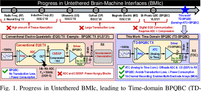
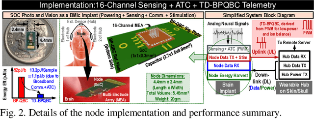
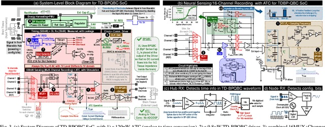
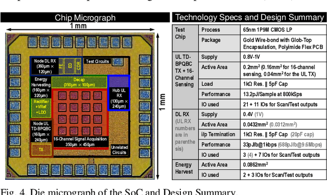
Abstract:Untethered miniaturized wireless neural sensor nodes with data transmission and energy harvesting capabilities call for circuit and system-level innovations to enable ultra-low energy deep implants for brain-machine interfaces. Realizing that the energy and size constraints of a neural implant motivate highly asymmetric system design (a small, low-power sensor and transmitter at the implant, with a relatively higher power receiver at a body-worn hub), we present Time-Domain Bi-Phasic Quasi-static Brain Communication (TD- BPQBC), offloading the burden of analog to digital conversion (ADC) and digital signal processing (DSP) to the receiver. The input analog signal is converted to time-domain pulse-width modulated (PWM) waveforms, and transmitted using the recently developed BPQBC method for reducing communication power in implants. The overall SoC consumes only 1.8{\mu}W power while sensing and communicating at 800kSps. The transmitter energy efficiency is only 1.1pJ/b, which is >30X better than the state-of-the-art, enabling a fully-electrical, energy-harvested, and connected in-brain sensor/stimulator node.
Bi-Phasic Quasistatic Brain Communication for Fully Untethered Connected Brain Implants
May 18, 2022Abstract:Wireless communication using electro-magnetic (EM) fields acts as the backbone for information exchange among wearable devices around the human body. However, for Implanted devices, EM fields incur high amount of absorption in the tissue, while alternative modes of transmission including ultrasound, optical and magneto-electric methods result in large amount of transduction losses due to conversion of one form of energy to another, thereby increasing the overall end-to-end energy loss. To solve the challenge of powering and communication in a brain implant with low end-end channel loss, we present Bi-Phasic Quasistatic Brain Communication (BP-QBC), achieving < 60dB worst-case end-to-end channel loss at a channel length of 55mm, by avoiding the transduction losses during field-modality conversion. BP-QBC utilizes dipole coupling based signal transmission within the brain tissue using differential excitation in the transmitter and differential signal pick-up at the receiver, and offers 41X lower power w.r.t. traditional Galvanic Human Body Communication at a carrier frequency of 1MHz, by blocking any DC current paths through the brain tissue. Since the electrical signal transfer through the human tissue is electro-quasistatic up to several 10's of MHz range, BP-QBC allows a scalable (bps-10Mbps) duty-cycled uplink from the implant to an external wearable. The power consumption in the BP-QBC TX is only 0.52uW at 1Mbps (with 1% duty cycling), which is within the range of harvested body-coupled power in the downlink from an external wearable to the brain implant. Furthermore, BP-QBC eliminates the need for sub-cranial repeaters, as it utilizes quasi-static electrical signals, thereby avoiding any transduction losses. Such low end-to-end channel loss with high data rates would find applications in neuroscience, brain-machine interfaces, electroceuticals and connected healthcare.
Channel Modeling for Physically Secure Electro-Quasistatic In-Body to Out-of-Body Communication with Galvanic Tx and Multimodal Rx
Apr 27, 2022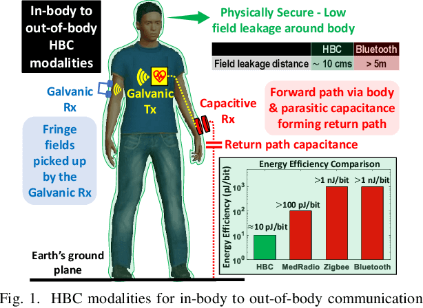
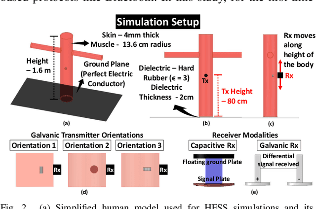

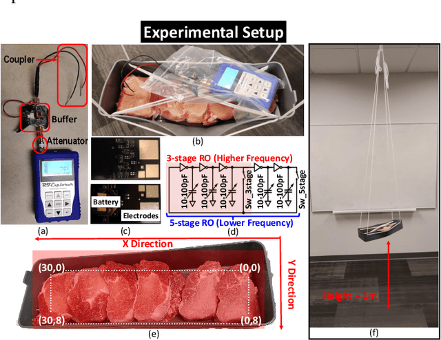
Abstract:Increasing number of devices being used in and around the human body has resulted in the exploration of the human body as a communication medium. In this paper, we design a channel model for implantable devices communicating outside the body using physically secure Electro-Quasistatic Human Body Communication. A galvanic receiver shows 5dB lower path loss than capacitive receiver when placed close to transmitter whereas a capacitive receiver has around 15dB lower path loss for larger separation between the transmitter and receiver. Finite Element Method (FEM) based simulations are used to analyze the communication channel for different receiver topologies and experimental data is used to validate the simulation results.
A Quantitative Analysis of Physical Security and Path Loss With Frequency for IBOB Channel
Apr 27, 2022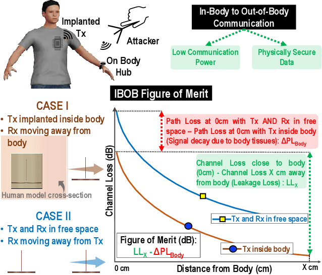
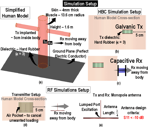

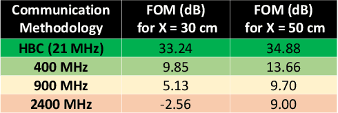
Abstract:Security vulnerabilities demonstrated in implantable medical devices have opened the door for research into physically secure and low power communication methodologies. In this study, we perform a comparative analysis of commonly used ISM frequency bands and human body communication (HBC) for data transfer from in-body to out-of-body (IBOB). We develop a figure of merit (FoM) that comprises of the critical parameters to quantitatively compare the communication methodologies. We perform finite-element method (FEM)-based simulations and experiments to validate the FoM developed.
EICO: Energy-Harvesting Long-Range Environmental Sensor Nodes with Energy-Information Dynamic Co-Optimization
Jul 15, 2021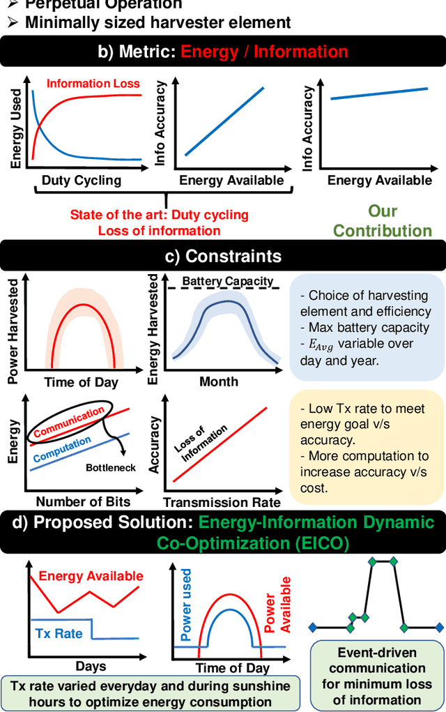
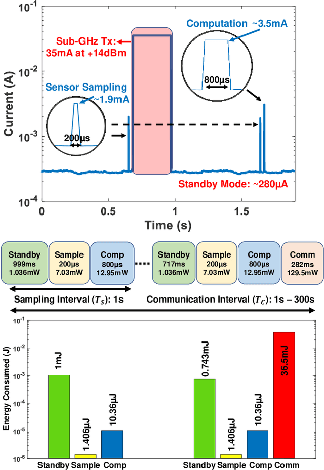
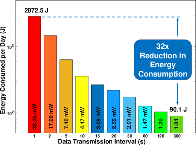
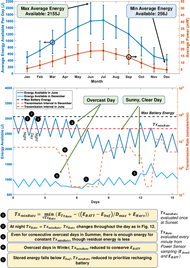
Abstract:Intensive research on energy harvested sensor nodes with traditional battery powered devices has been driven by the challenges in achieving the stringent design goals of battery lifetime, information accuracy, transmission distance, and cost. This challenge is further amplified by the inherent power intensive nature of long-range communication when sensor networks are required to span vast areas such as agricultural fields and remote terrain. Solar power is a common energy source is wireless sensor nodes, however, it is not reliable due to fluctuations in power stemming from the changing seasons and weather conditions. This paper tackles these issues by presenting a perpetually-powered, energy-harvesting sensor node which utilizes a minimally sized solar cell and is capable of long range communication by dynamically co-optimizing energy consumption and information transfer, termed as Energy-Information Dynamic Co-Optimization (EICO). This energy-information intelligence is achieved by adaptive duty cycling of information transfer based on the total amount of energy available from the harvester and charge storage element to optimize the energy consumption of the sensor node, while employing in-sensor analytics (ISA) to minimize loss of information. This is the first reported sensor node < 35cm2 in dimension, which is capable of long-range communication over > 1Km at continuous information transfer rates of upto 1 packet/second which is enabled by EICO and ISA.
A mmWave Oscillator Design Utilizing High-Q Active-Mode On-Chip MEMS Resonators for Improved Fundamental Limits of Phase Noise
Jul 05, 2021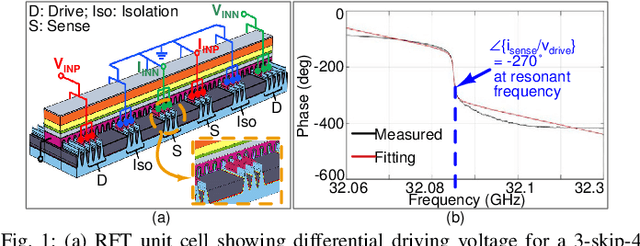
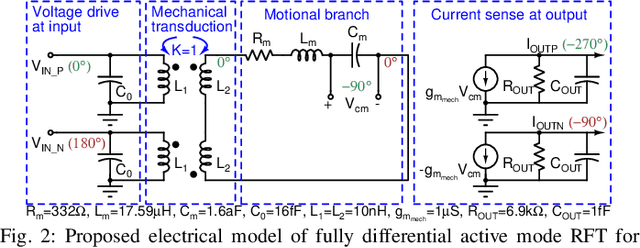
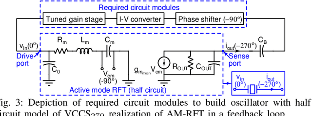
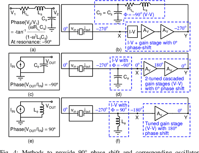
Abstract:(RFT) allows very high-Q active mode resonators, promising crystal-less monolithic clock generation for mmWave systems. However, there is a strong need for design of mmWave oscillators that utilize the high-Q of active-mode RFT (AM-RFT) optimally, while handling unique challenges such as resonator's low electromechanical transduction. In this brief, we develop a theory and through design and post-layout simulations in 14 nm Global Foundry process, we show the first active oscillator with AM-RFT at 30 GHz, which improves the fundamental limits of phase noise and figure-of-merit as compared to the oscillators with conventional LC resonators. For AM-RFT with Q factor of 10K, post layout simulation results show that the proposed oscillator exhibits phase noise less than -140 dBc per Hz and figure-of-merit greater than 228 dBc per Hz at 1 MHz offset for 30 GHz center frequency, which are more than 25 dB better than the existing monolithic LC oscillators.
OpenSerDes: An Open Source Process-Portable All-Digital Serial Link
May 27, 2021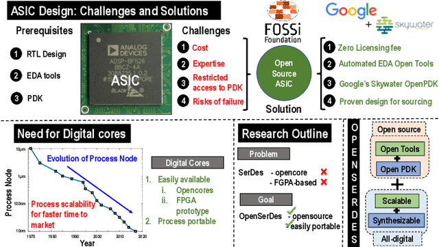
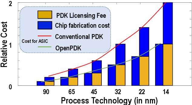

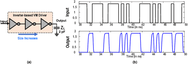
Abstract:In the last decade, the growing influence of open source software has necessitated the need to reduce the abstraction levels in hardware design. Open source hardware significantly reduces the development time, increasing the probability of first-pass success and enable developers to optimize software solutions based on hardware features, thereby reducing the design costs. The recent introduction of open source Process Development Kit (OpenPDK) by Skywater technologies in June 2020 has eliminated the barriers to Application-Specific Integrated Circuit (ASIC) design, which is otherwise considered expensive and not easily accessible. The OpenPDK is the first concrete step towards achieving the goal of open source circuit blocks that can be imported to reuse and modify in ASIC design. With process technologies scaling down for better performance, the need for entirely digital designs, which can be synthesized in any standard Automatic Place-and-Route (APR) tool, has increased considerably, for mapping physical design to the new process technology. This work presents the first open source all-digital Serializer/Deserializer (SerDes) for multi-GHz serial links designed using Skywater OpenPDK 130nm process node. To ensure that the design is fully synthesizable, the SerDes uses CMOS inverter-based drivers at the Tx, while the Rx front end comprises a resistive feedback inverter as a sensing element, followed by sampling elements. A fully digital oversampling CDR at the Rx recovers the Tx clock for proper decoding of data bits. The physical design flow utilizes OpenLANE, which is an end-to-end tool for generating GDS from RTL. Virtuoso has been used for extracting parasitics for post-layout simulations, which exhibit the SerDes functionality at 2 Gbps for 34 dB channel loss while consuming 438 mW power. The GDS and netlist files of the SerDes are uploaded in a GitHub repository for public access.
 Add to Chrome
 Add to Firefox
 Add to Edge