Gaurav Kumar K
Bi-Phasic Quasistatic Brain Communication for Fully Untethered Connected Brain Implants
May 18, 2022Abstract:Wireless communication using electro-magnetic (EM) fields acts as the backbone for information exchange among wearable devices around the human body. However, for Implanted devices, EM fields incur high amount of absorption in the tissue, while alternative modes of transmission including ultrasound, optical and magneto-electric methods result in large amount of transduction losses due to conversion of one form of energy to another, thereby increasing the overall end-to-end energy loss. To solve the challenge of powering and communication in a brain implant with low end-end channel loss, we present Bi-Phasic Quasistatic Brain Communication (BP-QBC), achieving < 60dB worst-case end-to-end channel loss at a channel length of 55mm, by avoiding the transduction losses during field-modality conversion. BP-QBC utilizes dipole coupling based signal transmission within the brain tissue using differential excitation in the transmitter and differential signal pick-up at the receiver, and offers 41X lower power w.r.t. traditional Galvanic Human Body Communication at a carrier frequency of 1MHz, by blocking any DC current paths through the brain tissue. Since the electrical signal transfer through the human tissue is electro-quasistatic up to several 10's of MHz range, BP-QBC allows a scalable (bps-10Mbps) duty-cycled uplink from the implant to an external wearable. The power consumption in the BP-QBC TX is only 0.52uW at 1Mbps (with 1% duty cycling), which is within the range of harvested body-coupled power in the downlink from an external wearable to the brain implant. Furthermore, BP-QBC eliminates the need for sub-cranial repeaters, as it utilizes quasi-static electrical signals, thereby avoiding any transduction losses. Such low end-to-end channel loss with high data rates would find applications in neuroscience, brain-machine interfaces, electroceuticals and connected healthcare.
OpenSerDes: An Open Source Process-Portable All-Digital Serial Link
May 27, 2021


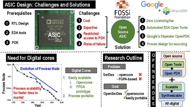
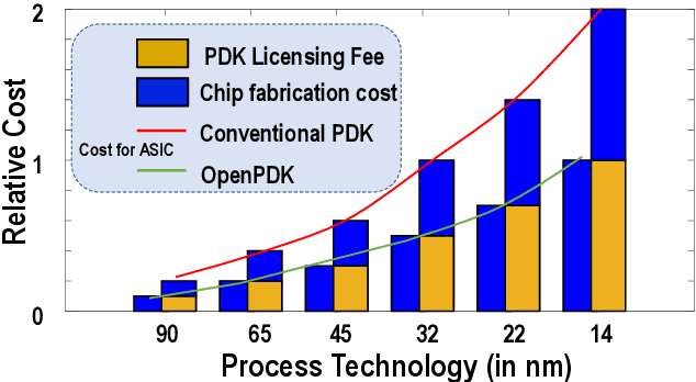
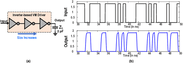
Abstract:In the last decade, the growing influence of open source software has necessitated the need to reduce the abstraction levels in hardware design. Open source hardware significantly reduces the development time, increasing the probability of first-pass success and enable developers to optimize software solutions based on hardware features, thereby reducing the design costs. The recent introduction of open source Process Development Kit (OpenPDK) by Skywater technologies in June 2020 has eliminated the barriers to Application-Specific Integrated Circuit (ASIC) design, which is otherwise considered expensive and not easily accessible. The OpenPDK is the first concrete step towards achieving the goal of open source circuit blocks that can be imported to reuse and modify in ASIC design. With process technologies scaling down for better performance, the need for entirely digital designs, which can be synthesized in any standard Automatic Place-and-Route (APR) tool, has increased considerably, for mapping physical design to the new process technology. This work presents the first open source all-digital Serializer/Deserializer (SerDes) for multi-GHz serial links designed using Skywater OpenPDK 130nm process node. To ensure that the design is fully synthesizable, the SerDes uses CMOS inverter-based drivers at the Tx, while the Rx front end comprises a resistive feedback inverter as a sensing element, followed by sampling elements. A fully digital oversampling CDR at the Rx recovers the Tx clock for proper decoding of data bits. The physical design flow utilizes OpenLANE, which is an end-to-end tool for generating GDS from RTL. Virtuoso has been used for extracting parasitics for post-layout simulations, which exhibit the SerDes functionality at 2 Gbps for 34 dB channel loss while consuming 438 mW power. The GDS and netlist files of the SerDes are uploaded in a GitHub repository for public access.
 Add to Chrome
 Add to Firefox
 Add to Edge