Shreyas Sen
From Muscle to Text with MyoText: sEMG to Text via Finger Classification and Transformer-Based Decoding
Jan 06, 2026Abstract:Surface electromyography (sEMG) provides a direct neural interface for decoding muscle activity and offers a promising foundation for keyboard-free text input in wearable and mixed-reality systems. Previous sEMG-to-text studies mainly focused on recognizing letters directly from sEMG signals, forming an important first step toward translating muscle activity into text. Building on this foundation, we present MyoText, a hierarchical framework that decodes sEMG signals to text through physiologically grounded intermediate stages. MyoText first classifies finger activations from multichannel sEMG using a CNN-BiLSTM-Attention model, applies ergonomic typing priors to infer letters, and reconstructs full sentences with a fine-tuned T5 transformer. This modular design mirrors the natural hierarchy of typing, linking muscle intent to language output and reducing the search space for decoding. Evaluated on 30 users from the emg2qwerty dataset, MyoText outperforms baselines by achieving 85.4% finger-classification accuracy, 5.4% character error rate (CER), and 6.5% word error rate (WER). Beyond accuracy gains, this methodology establishes a principled pathway from neuromuscular signals to text, providing a blueprint for virtual and augmented-reality typing interfaces that operate entirely without physical keyboards. By integrating ergonomic structure with transformer-based linguistic reasoning, MyoText advances the feasibility of seamless, wearable neural input for future ubiquitous computing environments.
Effect of nearby Metals on Electro-Quasistatic Human Body Communication
Oct 06, 2025Abstract:In recent decades Human Body Communication has emerged as a promising alternative to traditional radio wave communication, utilizing the body's conductive properties for low-power connectivity among wearables. This method harnesses the human body as an energy-efficient channel for data transmission within the electro-quasistatic frequency range, enabling advancements in human-machine interaction. While prior work has noted the role of parasitic return paths in such capacitively coupled systems, the influence of surrounding metallic objects on these paths, which are critical for EQS wireless signaling, has not been fully explored. This paper fills that gap with a structured study of how various conducting objects, from non-grounded (floating) metals and grounded metals to enclosed metallic environments such as elevators and cars, affect the body-communication channel. We present a theoretical framework supported by finite element method simulations and experiments with wearable devices. Results show that metallic objects within 20 cm of devices can reduce transmission loss by about 10 dB. When a device ground connects to a grounded metallic object, channel gain can increase by at least 20 dB. Contact area during touch-based interactions with grounded metals produces contact-impedance dependent high-pass channel characteristics. Proximity to metallic objects introduces variability within a critical distance, with grounded metals producing a larger overall effect than floating metals. These findings improve understanding of body-centric communication links and inform design for healthcare, consumer electronics, defense, and industrial applications.
Predicting and Understanding College Student Mental Health with Interpretable Machine Learning
Mar 11, 2025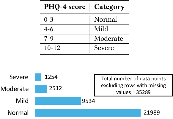
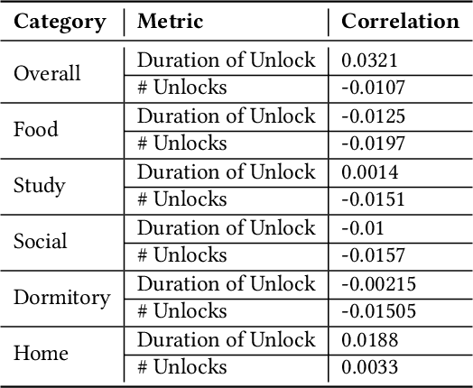
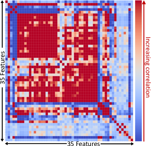
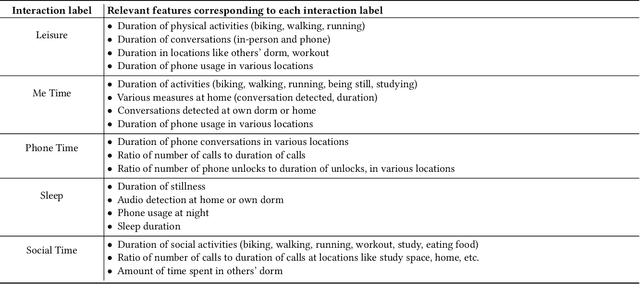
Abstract:Mental health issues among college students have reached critical levels, significantly impacting academic performance and overall wellbeing. Predicting and understanding mental health status among college students is challenging due to three main factors: the necessity for large-scale longitudinal datasets, the prevalence of black-box machine learning models lacking transparency, and the tendency of existing approaches to provide aggregated insights at the population level rather than individualized understanding. To tackle these challenges, this paper presents I-HOPE, the first Interpretable Hierarchical mOdel for Personalized mEntal health prediction. I-HOPE is a two-stage hierarchical model, validated on the College Experience Study, the longest longitudinal mobile sensing dataset. This dataset spans five years and captures data from both pre-pandemic periods and the COVID-19 pandemic. I-HOPE connects raw behavioral features to mental health status through five defined behavioral categories as interaction labels. This approach achieves a prediction accuracy of 91%, significantly surpassing the 60-70% accuracy of baseline methods. In addition, our model distills complex patterns into interpretable and individualized insights, enabling the future development of tailored interventions and improving mental health support. The code is available at https://github.com/roycmeghna/I-HOPE.
Body-Resonance Human Body Communication
Nov 16, 2024Abstract:Seamless interaction between Humans and AI-empowered battery-operated miniaturized electronic devices, exponentially transforming the wearable technology industry while forming an anthropomorphic artificial nervous system for distributed computing around the human body, demands high-speed low-power connectivity. If interconnected via radio frequency (RF) based wireless communication techniques, that being radiative, incur substantial absorption losses from the body during non-line-of-sight scenarios and consume higher power (more than 10s of mW). Although as a promising alternative with its non-radiative nature that resulted in 100X improvement in energy efficiency (sub-10 pJ/bit) and better signal confinement, Electro-Quasistatic Human Body Communication (EQS HBC) incurs moderate path loss (60-70 dB), limited data rate (less than 20 Mbps), making it less suitable for applications demanding fast connectivity like HD audio-video streaming, AR-VR-based products, distributed computing with wearable AI devices. Hence, to meet the requirement of energy-efficient connectivity at 100s of Mbps between wearables, we propose Body-Resonance (BR) HBC, which operates in the near-intermediate field and utilizes the transmission-line-like behavior of the body channel to offer 30X improvement in channel capacity. Our work sheds new light on the wireless communication system for wearables with potential to increase the channel gain by 20 dB with a 10X improvement in bandwidth compared to the EQS HBC for communication over on-body channels (whole-body coverage area). Experimentally demonstrating BR HBC, we presented low-loss (40-50 dB) and wide-band (hundreds of MHz) body channels that are 10X less leaky than radiative wireless communication, hence, can revolutionize the design of wireless communication system for several applications with wearables from healthcare, defense, to consumer electronics.
R-STELLAR: A Resilient Synthesizable Signature Attenuation SCA Protection on AES-256 with built-in Attack-on-Countermeasure Detection
Aug 21, 2024Abstract:Side channel attacks (SCAs) remain a significant threat to the security of cryptographic systems in modern embedded devices. Even mathematically secure cryptographic algorithms, when implemented in hardware, inadvertently leak information through physical side channel signatures such as power consumption, electromagnetic (EM) radiation, light emissions, and acoustic emanations. Exploiting these side channels significantly reduces the search space of the attacker. In recent years, physical countermeasures have significantly increased the minimum traces to disclosure (MTD) to 1 billion. Among them, signature attenuation is the first method to achieve this mark. Signature attenuation often relies on analog techniques, and digital signature attenuation reduces MTD to 20 million, requiring additional methods for high resilience. We focus on improving the digital signature attenuation by an order of magnitude (MTD 200M). Additionally, we explore possible attacks against signature attenuation countermeasure. We introduce a Voltage drop Linear region Biasing (VLB) attack technique that reduces the MTD to over 2000 times less than the previous threshold. This is the first known attack against a physical side-channel attack (SCA) countermeasure. We have implemented an attack detector with a response time of 0.8 milliseconds to detect such attacks, limiting SCA leakage window to sub-ms, which is insufficient for a successful attack.
Step-to-Charge: mW-scale power transfer to on-body devices for long channel (> 1m) with EQS Resonant Human Body Powering
Aug 04, 2024Abstract:Current limits of harvested energy in wearables are governed by three fundamental quantities, the physical limits of available energy density in ambient powering, safety limits in intentional powering, and the size of the wearable device. Typical energy harvested, except for solar power in favorable outdoor conditions, ranges from 5 uW to a maximum of 100 - 200 uW depending upon the available energy. Further, traditional intentional powering methodologies using ultrasound and radio-frequency either have a severe limitation in range of powering or are inefficient due to high path loss in Non-Line-of-Sight scenarios due to absorption by the body. In this study, we propose a novel approach using the human body, the common medium connecting the wearable devices, as a channel to transfer power. We demonstrate Human Body Powering using ``Step-to-Charge," a first-of-its-kind non-radiative, meter-scale powering methodology using a floor-based source and the human body as the channel to transfer power at lower channel losses to charge and power wearable devices across the whole body. The proposed powering methodology allows more than 2 mW peak power to be transferred to a wearable device for >1m channel lengths, which is > 90X greater than the state-of-the-art over previous Human Body Powering attempts. Step-to-Charge enables the powering of a new, extended range of wearable devices across the human body, bringing us closer to enabling battery-less perpetual operation using Human Body Power transfer.
Invited: Human-Inspired Distributed Wearable AI
Jun 26, 2024


Abstract:The explosive surge in Human-AI interactions, fused with a soaring fascination in wearable technology, has ignited a frenzy of innovation and the emergence of a myriad of Wearable AI devices, each wielding diverse form factors, tackling tasks from health surveillance to turbocharging productivity. This paper delves into the vision for wearable AI technology, addressing the technical bottlenecks that stand in the way of its promised advancements. Embracing a paradigm shift, we introduce a Human-Inspired Distributed Network for Wearable AI, enabled by high-speed ultra-low-power secure connectivity via the emerging 'Body as a Wire' (Wi-R) technology. This breakthrough acts as the missing link: the artificial nervous system, seamlessly interconnecting all wearables and implantables, ushering in a new era of interconnected intelligence, where featherweight, perpetually operating wearable AI nodes redefine the boundaries of possibility.
Approximate DCT and Quantization Techniques for Energy-Constrained Image Sensors
Jun 24, 2024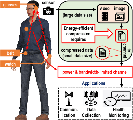
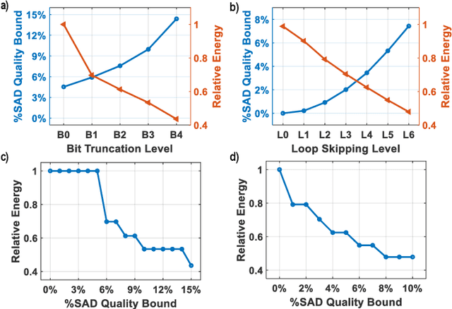
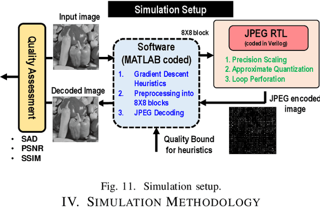
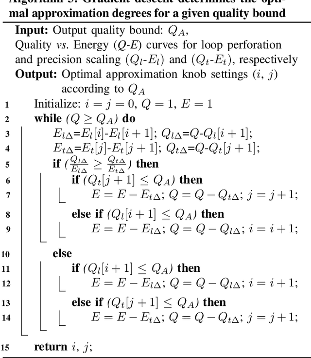
Abstract:Recent expansions in multimedia devices gather enormous amounts of real-time images for processing and inference. The images are first compressed using compression schemes, like JPEG, to reduce storage costs and power for transmitting the captured data. Due to inherent error resilience and imperceptibility in images, JPEG can be approximated to reduce the required computation power and area. This work demonstrates the first end-to-end approximation computing-based optimization of JPEG hardware using i) an approximate division realized using bit-shift operators to reduce the complexity of the quantization block, ii) loop perforation, and iii) precision scaling on top of a multiplier-less fast DCT architecture to achieve an extremely energy-efficient JPEG compression unit which will be a perfect fit for power/bandwidth-limited scenario. Furthermore, a gradient descent-based heuristic composed of two conventional approximation strategies, i.e., Precision Scaling and Loop Perforation, is implemented for tuning the degree of approximation to trade off energy consumption with the quality degradation of the decoded image. The entire RTL design is coded in Verilog HDL, synthesized, mapped to TSMC 65nm CMOS technology, and simulated using Cadence Spectre Simulator under 25$^{\circ}$\textbf{C}, TT corner. The approximate division approach achieved around $\textbf{28\%}$ reduction in the active design area. The heuristic-based approximation technique combined with accelerator optimization achieves a significant energy reduction of $\textbf{36\%}$ for a minimal image quality degradation of $\textbf{2\%}$ SAD. Simulation results also show that the proposed architecture consumes 15uW at the DCT and quantization stages to compress a colored 480p image at 6fps.
Efficient Communication and Powering for Smart Contact Lens with Resonant Magneto-Quasistatic Coupling
Jun 12, 2024


Abstract:A two-coil wearable system is proposed for wireless communication and powering between a transmitter coil in a necklace and a receiver coil in a smart contact lens, where the necklace is invisible in contrast to coils embedded in wearables like spectacles or headbands. Magneto-quasistatic(MQS) field coupling facilitates communication between the transmitter in the necklace and the contact lens receiver, enabling AR/VR and health monitoring. As long as the receiver coil remains within the magnetic field generated by the transmitter, continuous communication is sustained through MQS field coupling despite the misalignments present. Resonant frequency tuning enhances system efficiency. The system's performance was tested for coil misalignments, showing a maximum path loss variation within $10 dB$ across scenarios, indicating robustness. Finite Element Method(FEM) analysis has been used to study the system for efficient wireless data transfer and powering. A communication channel capacity is $4.5 Mbps$ over a $1 MHz$ bandwidth. Simulations show negligible path loss differences with or without human tissues, as magnetic coupling remains unaffected at MQS frequencies below $30 MHz$ due to similar magnetic permeability of tissues and air. Therefore, the possibility of efficient communication and powering of smart contact lenses through a necklace is shown for the first time using resonant MQS coupling at an axial distance of $15cm$ and lateral distance of over $9cm$ to enable AR/VR and health monitoring on the contact lens.
Invited: Can Wi-R enable perpetual IoB nodes?
Aug 08, 2023Abstract:While the number of wearables is steadily growing, the wearables/person wearing them faces a limitation due to the need for charging all of them every day. To unlock the true power of IoB, we need to make these IoB nodes perpetual. However, that is not possible with today's technology. In this paper, we will debate, whether with the advent of Wi-R protocol that uses the body to communicate at 100X lower energy that BTLE/Wi-Fi, is it going to be possible to enable the long-standing desire of perpetual sensing/actuation nodes for the Internet of Bodies.
 Add to Chrome
 Add to Firefox
 Add to Edge