Vic De Ridder
Addressing Class Imbalance and Data Limitations in Advanced Node Semiconductor Defect Inspection: A Generative Approach for SEM Images
Jul 14, 2024
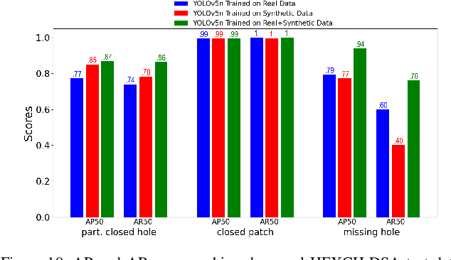
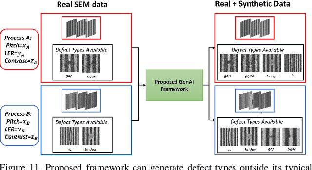

Abstract:Precision in identifying nanometer-scale device-killer defects is crucial in both semiconductor research and development as well as in production processes. The effectiveness of existing ML-based approaches in this context is largely limited by the scarcity of data, as the production of real semiconductor wafer data for training these models involves high financial and time costs. Moreover, the existing simulation methods fall short of replicating images with identical noise characteristics, surface roughness and stochastic variations at advanced nodes. We propose a method for generating synthetic semiconductor SEM images using a diffusion model within a limited data regime. In contrast to images generated through conventional simulation methods, SEM images generated through our proposed DL method closely resemble real SEM images, replicating their noise characteristics and surface roughness adaptively. Our main contributions, which are validated on three different real semiconductor datasets, are: i) proposing a patch-based generative framework utilizing DDPM to create SEM images with intended defect classes, addressing challenges related to class-imbalance and data insufficiency, ii) demonstrating generated synthetic images closely resemble real SEM images acquired from the tool, preserving all imaging conditions and metrology characteristics without any metadata supervision, iii) demonstrating a defect detector trained on generated defect dataset, either independently or combined with a limited real dataset, can achieve similar or improved performance on real wafer SEM images during validation/testing compared to exclusive training on a real defect dataset, iv) demonstrating the ability of the proposed approach to transfer defect types, critical dimensions, and imaging conditions from one specified CD/Pitch and metrology specifications to another, thereby highlighting its versatility.
Towards Improved Semiconductor Defect Inspection for high-NA EUVL based on SEMI-SuperYOLO-NAS
Apr 08, 2024Abstract:Due to potential pitch reduction, the semiconductor industry is adopting High-NA EUVL technology. However, its low depth of focus presents challenges for High Volume Manufacturing. To address this, suppliers are exploring thinner photoresists and new underlayers/hardmasks. These may suffer from poor SNR, complicating defect detection. Vision-based ML algorithms offer a promising solution for semiconductor defect inspection. However, developing a robust ML model across various image resolutions without explicit training remains a challenge for nano-scale defect inspection. This research's goal is to propose a scale-invariant ADCD framework capable to upscale images, addressing this issue. We propose an improvised ADCD framework as SEMI-SuperYOLO-NAS, which builds upon the baseline YOLO-NAS architecture. This framework integrates a SR assisted branch to aid in learning HR features by the defect detection backbone, particularly for detecting nano-scale defect instances from LR images. Additionally, the SR-assisted branch can recursively generate upscaled images from their corresponding downscaled counterparts, enabling defect detection inference across various image resolutions without requiring explicit training. Moreover, we investigate improved data augmentation strategy aimed at generating diverse and realistic training datasets to enhance model performance. We have evaluated our proposed approach using two original FAB datasets obtained from two distinct processes and captured using two different imaging tools. Finally, we demonstrate zero-shot inference for our model on a new, originating from a process condition distinct from the training dataset and possessing different Pitch characteristics. Experimental validation demonstrates that our proposed ADCD framework aids in increasing the throughput of imaging tools for defect inspection by reducing the required image pixel resolutions.
Improved Defect Detection and Classification Method for Advanced IC Nodes by Using Slicing Aided Hyper Inference with Refinement Strategy
Nov 21, 2023
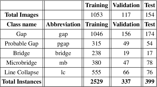
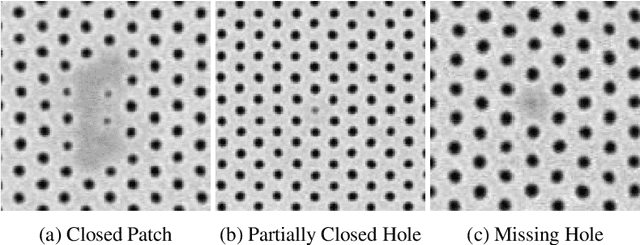
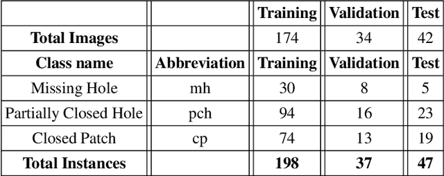
Abstract:In semiconductor manufacturing, lithography has often been the manufacturing step defining the smallest possible pattern dimensions. In recent years, progress has been made towards high-NA (Numerical Aperture) EUVL (Extreme-Ultraviolet-Lithography) paradigm, which promises to advance pattern shrinking (2 nm node and beyond). However, a significant increase in stochastic defects and the complexity of defect detection becomes more pronounced with high-NA. Present defect inspection techniques (both non-machine learning and machine learning based), fail to achieve satisfactory performance at high-NA dimensions. In this work, we investigate the use of the Slicing Aided Hyper Inference (SAHI) framework for improving upon current techniques. Using SAHI, inference is performed on size-increased slices of the SEM images. This leads to the object detector's receptive field being more effective in capturing small defect instances. First, the performance on previously investigated semiconductor datasets is benchmarked across various configurations, and the SAHI approach is demonstrated to substantially enhance the detection of small defects, by approx. 2x. Afterwards, we also demonstrated application of SAHI leads to flawless detection rates on a new test dataset, with scenarios not encountered during training, whereas previous trained models failed. Finally, we formulate an extension of SAHI that does not significantly reduce true-positive predictions while eliminating false-positive predictions.
SEMI-CenterNet: A Machine Learning Facilitated Approach for Semiconductor Defect Inspection
Aug 15, 2023Abstract:Continual shrinking of pattern dimensions in the semiconductor domain is making it increasingly difficult to inspect defects due to factors such as the presence of stochastic noise and the dynamic behavior of defect patterns and types. Conventional rule-based methods and non-parametric supervised machine learning algorithms like KNN mostly fail at the requirements of semiconductor defect inspection at these advanced nodes. Deep Learning (DL)-based methods have gained popularity in the semiconductor defect inspection domain because they have been proven robust towards these challenging scenarios. In this research work, we have presented an automated DL-based approach for efficient localization and classification of defects in SEM images. We have proposed SEMI-CenterNet (SEMI-CN), a customized CN architecture trained on SEM images of semiconductor wafer defects. The use of the proposed CN approach allows improved computational efficiency compared to previously studied DL models. SEMI-CN gets trained to output the center, class, size, and offset of a defect instance. This is different from the approach of most object detection models that use anchors for bounding box prediction. Previous methods predict redundant bounding boxes, most of which are discarded in postprocessing. CN mitigates this by only predicting boxes for likely defect center points. We train SEMI-CN on two datasets and benchmark two ResNet backbones for the framework. Initially, ResNet models pretrained on the COCO dataset undergo training using two datasets separately. Primarily, SEMI-CN shows significant improvement in inference time against previous research works. Finally, transfer learning (using weights of custom SEM dataset) is applied from ADI dataset to AEI dataset and vice-versa, which reduces the required training time for both backbones to reach the best mAP against conventional training method.
SEMI-DiffusionInst: A Diffusion Model Based Approach for Semiconductor Defect Classification and Segmentation
Jul 17, 2023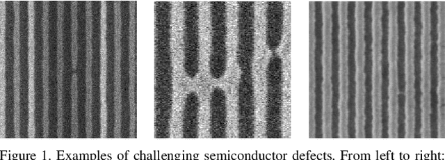

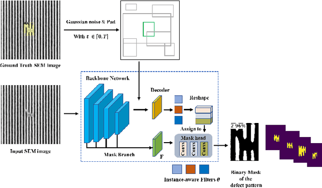
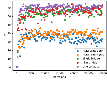
Abstract:With continuous progression of Moore's Law, integrated circuit (IC) device complexity is also increasing. Scanning Electron Microscope (SEM) image based extensive defect inspection and accurate metrology extraction are two main challenges in advanced node (2 nm and beyond) technology. Deep learning (DL) algorithm based computer vision approaches gained popularity in semiconductor defect inspection over last few years. In this research work, a new semiconductor defect inspection framework "SEMI-DiffusionInst" is investigated and compared to previous frameworks. To the best of the authors' knowledge, this work is the first demonstration to accurately detect and precisely segment semiconductor defect patterns by using a diffusion model. Different feature extractor networks as backbones and data sampling strategies are investigated towards achieving a balanced trade-off between precision and computing efficiency. Our proposed approach outperforms previous work on overall mAP and performs comparatively better or as per for almost all defect classes (per class APs). The bounding box and segmentation mAPs achieved by the proposed SEMI-DiffusionInst model are improved by 3.83% and 2.10%,respectively. Among individual defect types, precision on line collapse and thin bridge defects are improved approximately 15% on detection task for both defect types. It has also been shown that by tuning inference hyperparameters, inference time can be improved significantly without compromising model precision. Finally, certain limitations and future work strategy to overcome them are discussed.
 Add to Chrome
 Add to Firefox
 Add to Edge