Sandip Halder
Unsupervised Anomaly Prediction with N-BEATS and Graph Neural Network in Multi-variate Semiconductor Process Time Series
Oct 23, 2025Abstract:Semiconductor manufacturing is an extremely complex and precision-driven process, characterized by thousands of interdependent parameters collected across diverse tools and process steps. Multi-variate time-series analysis has emerged as a critical field for real-time monitoring and fault detection in such environments. However, anomaly prediction in semiconductor fabrication presents several critical challenges, including high dimensionality of sensor data and severe class imbalance due to the rarity of true faults. Furthermore, the complex interdependencies between variables complicate both anomaly prediction and root-cause-analysis. This paper proposes two novel approaches to advance the field from anomaly detection to anomaly prediction, an essential step toward enabling real-time process correction and proactive fault prevention. The proposed anomaly prediction framework contains two main stages: (a) training a forecasting model on a dataset assumed to contain no anomalies, and (b) performing forecast on unseen time series data. The forecast is compared with the forecast of the trained signal. Deviations beyond a predefined threshold are flagged as anomalies. The two approaches differ in the forecasting model employed. The first assumes independence between variables by utilizing the N-BEATS model for univariate time series forecasting. The second lifts this assumption by utilizing a Graph Neural Network (GNN) to capture inter-variable relationships. Both models demonstrate strong forecasting performance up to a horizon of 20 time points and maintain stable anomaly prediction up to 50 time points. The GNN consistently outperforms the N-BEATS model while requiring significantly fewer trainable parameters and lower computational cost. These results position the GNN as promising solution for online anomaly forecasting to be deployed in manufacturing environments.
Advancing SEM Based Nano-Scale Defect Analysis in Semiconductor Manufacturing for Advanced IC Nodes
Sep 06, 2024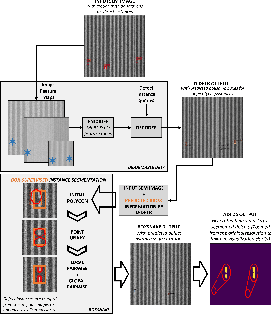

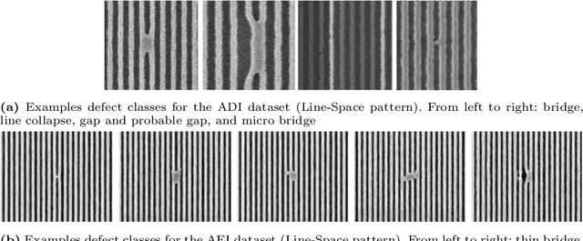
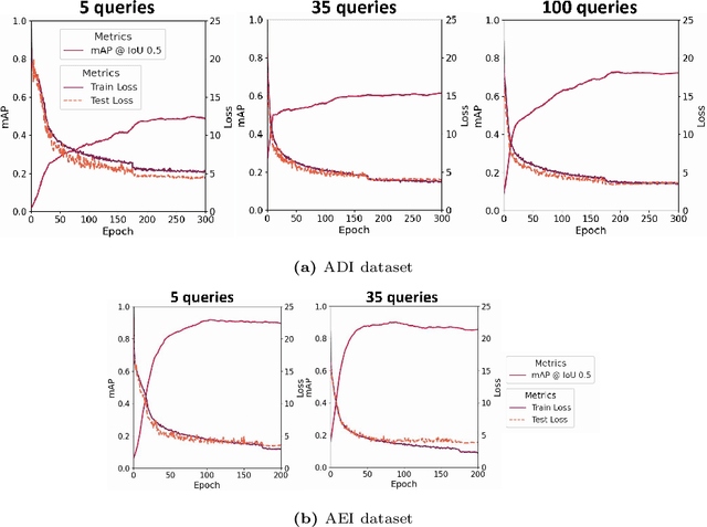
Abstract:In this research, we introduce a unified end-to-end Automated Defect Classification-Detection-Segmentation (ADCDS) framework for classifying, detecting, and segmenting multiple instances of semiconductor defects for advanced nodes. This framework consists of two modules: (a) a defect detection module, followed by (b) a defect segmentation module. The defect detection module employs Deformable DETR to aid in the classification and detection of nano-scale defects, while the segmentation module utilizes BoxSnake. BoxSnake facilitates box-supervised instance segmentation of nano-scale defects, supported by the former module. This simplifies the process by eliminating the laborious requirement for ground-truth pixel-wise mask annotation by human experts, which is typically associated with training conventional segmentation models. We have evaluated the performance of our ADCDS framework using two distinct process datasets from real wafers, as ADI and AEI, specifically focusing on Line-space patterns. We have demonstrated the applicability and significance of our proposed methodology, particularly in the nano-scale segmentation and generation of binary defect masks, using the challenging ADI SEM dataset where ground-truth pixelwise segmentation annotations were unavailable. Furthermore, we have presented a comparative analysis of our proposed framework against previous approaches to demonstrate its effectiveness. Our proposed framework achieved an overall mAP@IoU0.5 of 72.19 for detection and 78.86 for segmentation on the ADI dataset. Similarly, for the AEI dataset, these metrics were 90.38 for detection and 95.48 for segmentation. Thus, our proposed framework effectively fulfils the requirements of advanced defect analysis while addressing significant constraints.
An Evaluation of Continual Learning for Advanced Node Semiconductor Defect Inspection
Jul 17, 2024


Abstract:Deep learning-based semiconductor defect inspection has gained traction in recent years, offering a powerful and versatile approach that provides high accuracy, adaptability, and efficiency in detecting and classifying nano-scale defects. However, semiconductor manufacturing processes are continually evolving, leading to the emergence of new types of defects over time. This presents a significant challenge for conventional supervised defect detectors, as they may suffer from catastrophic forgetting when trained on new defect datasets, potentially compromising performance on previously learned tasks. An alternative approach involves the constant storage of previously trained datasets alongside pre-trained model versions, which can be utilized for (re-)training from scratch or fine-tuning whenever encountering a new defect dataset. However, adhering to such a storage template is impractical in terms of size, particularly when considering High-Volume Manufacturing (HVM). Additionally, semiconductor defect datasets, especially those encompassing stochastic defects, are often limited and expensive to obtain, thus lacking sufficient representation of the entire universal set of defectivity. This work introduces a task-agnostic, meta-learning approach aimed at addressing this challenge, which enables the incremental addition of new defect classes and scales to create a more robust and generalized model for semiconductor defect inspection. We have benchmarked our approach using real resist-wafer SEM (Scanning Electron Microscopy) datasets for two process steps, ADI and AEI, demonstrating its superior performance compared to conventional supervised training methods.
Addressing Class Imbalance and Data Limitations in Advanced Node Semiconductor Defect Inspection: A Generative Approach for SEM Images
Jul 14, 2024
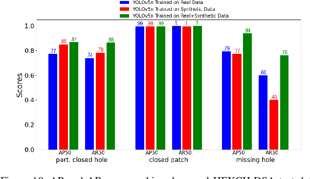
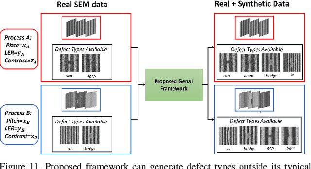

Abstract:Precision in identifying nanometer-scale device-killer defects is crucial in both semiconductor research and development as well as in production processes. The effectiveness of existing ML-based approaches in this context is largely limited by the scarcity of data, as the production of real semiconductor wafer data for training these models involves high financial and time costs. Moreover, the existing simulation methods fall short of replicating images with identical noise characteristics, surface roughness and stochastic variations at advanced nodes. We propose a method for generating synthetic semiconductor SEM images using a diffusion model within a limited data regime. In contrast to images generated through conventional simulation methods, SEM images generated through our proposed DL method closely resemble real SEM images, replicating their noise characteristics and surface roughness adaptively. Our main contributions, which are validated on three different real semiconductor datasets, are: i) proposing a patch-based generative framework utilizing DDPM to create SEM images with intended defect classes, addressing challenges related to class-imbalance and data insufficiency, ii) demonstrating generated synthetic images closely resemble real SEM images acquired from the tool, preserving all imaging conditions and metrology characteristics without any metadata supervision, iii) demonstrating a defect detector trained on generated defect dataset, either independently or combined with a limited real dataset, can achieve similar or improved performance on real wafer SEM images during validation/testing compared to exclusive training on a real defect dataset, iv) demonstrating the ability of the proposed approach to transfer defect types, critical dimensions, and imaging conditions from one specified CD/Pitch and metrology specifications to another, thereby highlighting its versatility.
Towards Improved Semiconductor Defect Inspection for high-NA EUVL based on SEMI-SuperYOLO-NAS
Apr 08, 2024Abstract:Due to potential pitch reduction, the semiconductor industry is adopting High-NA EUVL technology. However, its low depth of focus presents challenges for High Volume Manufacturing. To address this, suppliers are exploring thinner photoresists and new underlayers/hardmasks. These may suffer from poor SNR, complicating defect detection. Vision-based ML algorithms offer a promising solution for semiconductor defect inspection. However, developing a robust ML model across various image resolutions without explicit training remains a challenge for nano-scale defect inspection. This research's goal is to propose a scale-invariant ADCD framework capable to upscale images, addressing this issue. We propose an improvised ADCD framework as SEMI-SuperYOLO-NAS, which builds upon the baseline YOLO-NAS architecture. This framework integrates a SR assisted branch to aid in learning HR features by the defect detection backbone, particularly for detecting nano-scale defect instances from LR images. Additionally, the SR-assisted branch can recursively generate upscaled images from their corresponding downscaled counterparts, enabling defect detection inference across various image resolutions without requiring explicit training. Moreover, we investigate improved data augmentation strategy aimed at generating diverse and realistic training datasets to enhance model performance. We have evaluated our proposed approach using two original FAB datasets obtained from two distinct processes and captured using two different imaging tools. Finally, we demonstrate zero-shot inference for our model on a new, originating from a process condition distinct from the training dataset and possessing different Pitch characteristics. Experimental validation demonstrates that our proposed ADCD framework aids in increasing the throughput of imaging tools for defect inspection by reducing the required image pixel resolutions.
Improved Defect Detection and Classification Method for Advanced IC Nodes by Using Slicing Aided Hyper Inference with Refinement Strategy
Nov 21, 2023
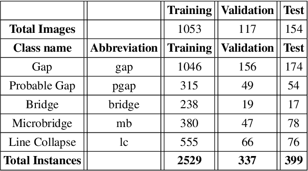
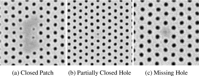
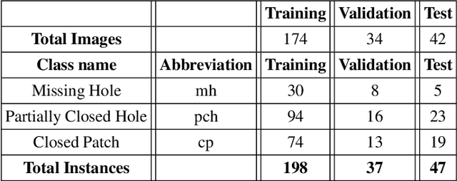
Abstract:In semiconductor manufacturing, lithography has often been the manufacturing step defining the smallest possible pattern dimensions. In recent years, progress has been made towards high-NA (Numerical Aperture) EUVL (Extreme-Ultraviolet-Lithography) paradigm, which promises to advance pattern shrinking (2 nm node and beyond). However, a significant increase in stochastic defects and the complexity of defect detection becomes more pronounced with high-NA. Present defect inspection techniques (both non-machine learning and machine learning based), fail to achieve satisfactory performance at high-NA dimensions. In this work, we investigate the use of the Slicing Aided Hyper Inference (SAHI) framework for improving upon current techniques. Using SAHI, inference is performed on size-increased slices of the SEM images. This leads to the object detector's receptive field being more effective in capturing small defect instances. First, the performance on previously investigated semiconductor datasets is benchmarked across various configurations, and the SAHI approach is demonstrated to substantially enhance the detection of small defects, by approx. 2x. Afterwards, we also demonstrated application of SAHI leads to flawless detection rates on a new test dataset, with scenarios not encountered during training, whereas previous trained models failed. Finally, we formulate an extension of SAHI that does not significantly reduce true-positive predictions while eliminating false-positive predictions.
Benchmarking Feature Extractors for Reinforcement Learning-Based Semiconductor Defect Localization
Nov 18, 2023


Abstract:As semiconductor patterning dimensions shrink, more advanced Scanning Electron Microscopy (SEM) image-based defect inspection techniques are needed. Recently, many Machine Learning (ML)-based approaches have been proposed for defect localization and have shown impressive results. These methods often rely on feature extraction from a full SEM image and possibly a number of regions of interest. In this study, we propose a deep Reinforcement Learning (RL)-based approach to defect localization which iteratively extracts features from increasingly smaller regions of the input image. We compare the results of 18 agents trained with different feature extractors. We discuss the advantages and disadvantages of different feature extractors as well as the RL-based framework in general for semiconductor defect localization.
* 5 pages, 5 figures, 3 tables
Deep learning denoiser assisted roughness measurements extraction from thin resists with low Signal-to-Noise Ratio(SNR) SEM images: analysis with SMILE
Oct 23, 2023Abstract:The technological advance of High Numerical Aperture Extreme Ultraviolet Lithography (High NA EUVL) has opened the gates to extensive researches on thinner photoresists (below 30nm), necessary for the industrial implementation of High NA EUVL. Consequently, images from Scanning Electron Microscopy (SEM) suffer from reduced imaging contrast and low Signal-to-Noise Ratio (SNR), impacting the measurement of unbiased Line Edge Roughness (uLER) and Line Width Roughness (uLWR). Thus, the aim of this work is to enhance the SNR of SEM images by using a Deep Learning denoiser and enable robust roughness extraction of the thin resist. For this study, we acquired SEM images of Line-Space (L/S) patterns with a Chemically Amplified Resist (CAR) with different thicknesses (15nm, 20nm, 25nm, 30nm), underlayers (Spin-On-Glass-SOG, Organic Underlayer-OUL) and frames of averaging (4, 8, 16, 32, and 64 Fr). After denoising, a systematic analysis has been carried out on both noisy and denoised images using an open-source metrology software, SMILE 2.3.2, for investigating mean CD, SNR improvement factor, biased and unbiased LWR/LER Power Spectral Density (PSD). Denoised images with lower number of frames present unaltered Critical Dimensions (CDs), enhanced SNR (especially for low number of integration frames), and accurate measurements of uLER and uLWR, with the same accuracy as for noisy images with a consistent higher number of frames. Therefore, images with a small number of integration frames and with SNR < 2 can be successfully denoised, and advantageously used in improving metrology throughput while maintaining reliable roughness measurements for the thin resist.
Automated Semiconductor Defect Inspection in Scanning Electron Microscope Images: a Systematic Review
Aug 18, 2023


Abstract:A growing need exists for efficient and accurate methods for detecting defects in semiconductor materials and devices. These defects can have a detrimental impact on the efficiency of the manufacturing process, because they cause critical failures and wafer-yield limitations. As nodes and patterns get smaller, even high-resolution imaging techniques such as Scanning Electron Microscopy (SEM) produce noisy images due to operating close to sensitivity levels and due to varying physical properties of different underlayers or resist materials. This inherent noise is one of the main challenges for defect inspection. One promising approach is the use of machine learning algorithms, which can be trained to accurately classify and locate defects in semiconductor samples. Recently, convolutional neural networks have proved to be particularly useful in this regard. This systematic review provides a comprehensive overview of the state of automated semiconductor defect inspection on SEM images, including the most recent innovations and developments. 38 publications were selected on this topic, indexed in IEEE Xplore and SPIE databases. For each of these, the application, methodology, dataset, results, limitations and future work were summarized. A comprehensive overview and analysis of their methods is provided. Finally, promising avenues for future work in the field of SEM-based defect inspection are suggested.
SEMI-CenterNet: A Machine Learning Facilitated Approach for Semiconductor Defect Inspection
Aug 15, 2023Abstract:Continual shrinking of pattern dimensions in the semiconductor domain is making it increasingly difficult to inspect defects due to factors such as the presence of stochastic noise and the dynamic behavior of defect patterns and types. Conventional rule-based methods and non-parametric supervised machine learning algorithms like KNN mostly fail at the requirements of semiconductor defect inspection at these advanced nodes. Deep Learning (DL)-based methods have gained popularity in the semiconductor defect inspection domain because they have been proven robust towards these challenging scenarios. In this research work, we have presented an automated DL-based approach for efficient localization and classification of defects in SEM images. We have proposed SEMI-CenterNet (SEMI-CN), a customized CN architecture trained on SEM images of semiconductor wafer defects. The use of the proposed CN approach allows improved computational efficiency compared to previously studied DL models. SEMI-CN gets trained to output the center, class, size, and offset of a defect instance. This is different from the approach of most object detection models that use anchors for bounding box prediction. Previous methods predict redundant bounding boxes, most of which are discarded in postprocessing. CN mitigates this by only predicting boxes for likely defect center points. We train SEMI-CN on two datasets and benchmark two ResNet backbones for the framework. Initially, ResNet models pretrained on the COCO dataset undergo training using two datasets separately. Primarily, SEMI-CN shows significant improvement in inference time against previous research works. Finally, transfer learning (using weights of custom SEM dataset) is applied from ADI dataset to AEI dataset and vice-versa, which reduces the required training time for both backbones to reach the best mAP against conventional training method.
 Add to Chrome
 Add to Firefox
 Add to Edge