Addressing Class Imbalance and Data Limitations in Advanced Node Semiconductor Defect Inspection: A Generative Approach for SEM Images
Paper and Code
Jul 14, 2024


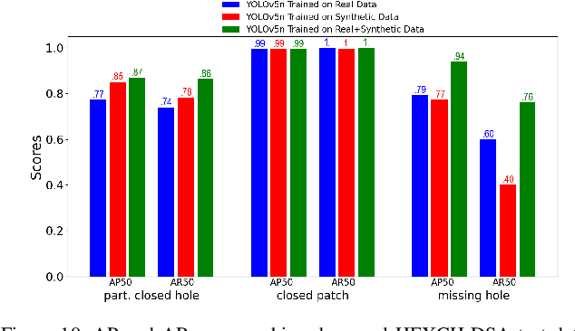
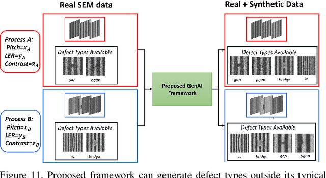
Precision in identifying nanometer-scale device-killer defects is crucial in both semiconductor research and development as well as in production processes. The effectiveness of existing ML-based approaches in this context is largely limited by the scarcity of data, as the production of real semiconductor wafer data for training these models involves high financial and time costs. Moreover, the existing simulation methods fall short of replicating images with identical noise characteristics, surface roughness and stochastic variations at advanced nodes. We propose a method for generating synthetic semiconductor SEM images using a diffusion model within a limited data regime. In contrast to images generated through conventional simulation methods, SEM images generated through our proposed DL method closely resemble real SEM images, replicating their noise characteristics and surface roughness adaptively. Our main contributions, which are validated on three different real semiconductor datasets, are: i) proposing a patch-based generative framework utilizing DDPM to create SEM images with intended defect classes, addressing challenges related to class-imbalance and data insufficiency, ii) demonstrating generated synthetic images closely resemble real SEM images acquired from the tool, preserving all imaging conditions and metrology characteristics without any metadata supervision, iii) demonstrating a defect detector trained on generated defect dataset, either independently or combined with a limited real dataset, can achieve similar or improved performance on real wafer SEM images during validation/testing compared to exclusive training on a real defect dataset, iv) demonstrating the ability of the proposed approach to transfer defect types, critical dimensions, and imaging conditions from one specified CD/Pitch and metrology specifications to another, thereby highlighting its versatility.
 Add to Chrome
 Add to Firefox
 Add to Edge