Stefan De Gendt
Advancing SEM Based Nano-Scale Defect Analysis in Semiconductor Manufacturing for Advanced IC Nodes
Sep 06, 2024


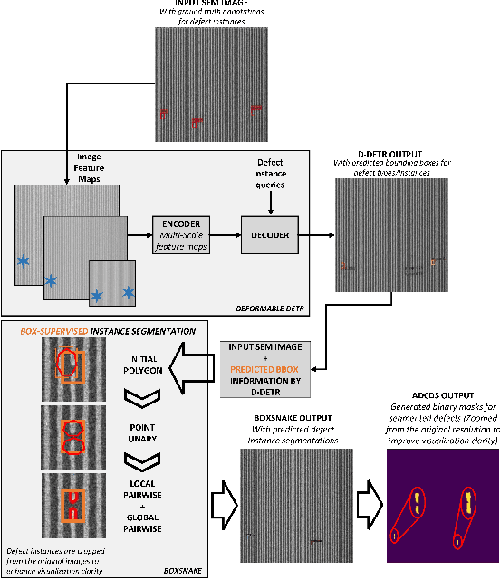
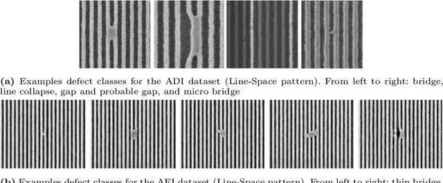
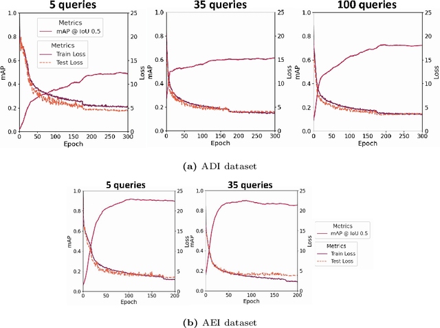
Abstract:In this research, we introduce a unified end-to-end Automated Defect Classification-Detection-Segmentation (ADCDS) framework for classifying, detecting, and segmenting multiple instances of semiconductor defects for advanced nodes. This framework consists of two modules: (a) a defect detection module, followed by (b) a defect segmentation module. The defect detection module employs Deformable DETR to aid in the classification and detection of nano-scale defects, while the segmentation module utilizes BoxSnake. BoxSnake facilitates box-supervised instance segmentation of nano-scale defects, supported by the former module. This simplifies the process by eliminating the laborious requirement for ground-truth pixel-wise mask annotation by human experts, which is typically associated with training conventional segmentation models. We have evaluated the performance of our ADCDS framework using two distinct process datasets from real wafers, as ADI and AEI, specifically focusing on Line-space patterns. We have demonstrated the applicability and significance of our proposed methodology, particularly in the nano-scale segmentation and generation of binary defect masks, using the challenging ADI SEM dataset where ground-truth pixelwise segmentation annotations were unavailable. Furthermore, we have presented a comparative analysis of our proposed framework against previous approaches to demonstrate its effectiveness. Our proposed framework achieved an overall mAP@IoU0.5 of 72.19 for detection and 78.86 for segmentation on the ADI dataset. Similarly, for the AEI dataset, these metrics were 90.38 for detection and 95.48 for segmentation. Thus, our proposed framework effectively fulfils the requirements of advanced defect analysis while addressing significant constraints.
Benchmarking Feature Extractors for Reinforcement Learning-Based Semiconductor Defect Localization
Nov 18, 2023


Abstract:As semiconductor patterning dimensions shrink, more advanced Scanning Electron Microscopy (SEM) image-based defect inspection techniques are needed. Recently, many Machine Learning (ML)-based approaches have been proposed for defect localization and have shown impressive results. These methods often rely on feature extraction from a full SEM image and possibly a number of regions of interest. In this study, we propose a deep Reinforcement Learning (RL)-based approach to defect localization which iteratively extracts features from increasingly smaller regions of the input image. We compare the results of 18 agents trained with different feature extractors. We discuss the advantages and disadvantages of different feature extractors as well as the RL-based framework in general for semiconductor defect localization.
* 5 pages, 5 figures, 3 tables
Automated Semiconductor Defect Inspection in Scanning Electron Microscope Images: a Systematic Review
Aug 18, 2023Abstract:A growing need exists for efficient and accurate methods for detecting defects in semiconductor materials and devices. These defects can have a detrimental impact on the efficiency of the manufacturing process, because they cause critical failures and wafer-yield limitations. As nodes and patterns get smaller, even high-resolution imaging techniques such as Scanning Electron Microscopy (SEM) produce noisy images due to operating close to sensitivity levels and due to varying physical properties of different underlayers or resist materials. This inherent noise is one of the main challenges for defect inspection. One promising approach is the use of machine learning algorithms, which can be trained to accurately classify and locate defects in semiconductor samples. Recently, convolutional neural networks have proved to be particularly useful in this regard. This systematic review provides a comprehensive overview of the state of automated semiconductor defect inspection on SEM images, including the most recent innovations and developments. 38 publications were selected on this topic, indexed in IEEE Xplore and SPIE databases. For each of these, the application, methodology, dataset, results, limitations and future work were summarized. A comprehensive overview and analysis of their methods is provided. Finally, promising avenues for future work in the field of SEM-based defect inspection are suggested.
SEMI-CenterNet: A Machine Learning Facilitated Approach for Semiconductor Defect Inspection
Aug 15, 2023Abstract:Continual shrinking of pattern dimensions in the semiconductor domain is making it increasingly difficult to inspect defects due to factors such as the presence of stochastic noise and the dynamic behavior of defect patterns and types. Conventional rule-based methods and non-parametric supervised machine learning algorithms like KNN mostly fail at the requirements of semiconductor defect inspection at these advanced nodes. Deep Learning (DL)-based methods have gained popularity in the semiconductor defect inspection domain because they have been proven robust towards these challenging scenarios. In this research work, we have presented an automated DL-based approach for efficient localization and classification of defects in SEM images. We have proposed SEMI-CenterNet (SEMI-CN), a customized CN architecture trained on SEM images of semiconductor wafer defects. The use of the proposed CN approach allows improved computational efficiency compared to previously studied DL models. SEMI-CN gets trained to output the center, class, size, and offset of a defect instance. This is different from the approach of most object detection models that use anchors for bounding box prediction. Previous methods predict redundant bounding boxes, most of which are discarded in postprocessing. CN mitigates this by only predicting boxes for likely defect center points. We train SEMI-CN on two datasets and benchmark two ResNet backbones for the framework. Initially, ResNet models pretrained on the COCO dataset undergo training using two datasets separately. Primarily, SEMI-CN shows significant improvement in inference time against previous research works. Finally, transfer learning (using weights of custom SEM dataset) is applied from ADI dataset to AEI dataset and vice-versa, which reduces the required training time for both backbones to reach the best mAP against conventional training method.
YOLOv8 for Defect Inspection of Hexagonal Directed Self-Assembly Patterns: A Data-Centric Approach
Jul 28, 2023Abstract:Shrinking pattern dimensions leads to an increased variety of defect types in semiconductor devices. This has spurred innovation in patterning approaches such as Directed self-assembly (DSA) for which no traditional, automatic defect inspection software exists. Machine Learning-based SEM image analysis has become an increasingly popular research topic for defect inspection with supervised ML models often showing the best performance. However, little research has been done on obtaining a dataset with high-quality labels for these supervised models. In this work, we propose a method for obtaining coherent and complete labels for a dataset of hexagonal contact hole DSA patterns while requiring minimal quality control effort from a DSA expert. We show that YOLOv8, a state-of-the-art neural network, achieves defect detection precisions of more than 0.9 mAP on our final dataset which best reflects DSA expert defect labeling expectations. We discuss the strengths and limitations of our proposed labeling approach and suggest directions for future work in data-centric ML-based defect inspection.
A Deep Learning Framework for Verilog Autocompletion Towards Design and Verification Automation
Apr 26, 2023Abstract:Innovative Electronic Design Automation (EDA) solutions are important to meet the design requirements for increasingly complex electronic devices. Verilog, a hardware description language, is widely used for the design and verification of digital circuits and is synthesized using specific EDA tools. However, writing code is a repetitive and time-intensive task. This paper proposes, primarily, a novel deep learning framework for training a Verilog autocompletion model and, secondarily, a Verilog dataset of files and snippets obtained from open-source repositories. The framework involves integrating models pretrained on general programming language data and finetuning them on a dataset curated to be similar to a target downstream task. This is validated by comparing different pretrained models trained on different subsets of the proposed Verilog dataset using multiple evaluation metrics. These experiments demonstrate that the proposed framework achieves better BLEU, ROUGE-L, and chrF scores by 9.5%, 6.7%, and 6.9%, respectively, compared to a model trained from scratch.
Optimizing YOLOv7 for Semiconductor Defect Detection
Feb 19, 2023Abstract:The field of object detection using Deep Learning (DL) is constantly evolving with many new techniques and models being proposed. YOLOv7 is a state-of-the-art object detector based on the YOLO family of models which have become popular for industrial applications. One such possible application domain can be semiconductor defect inspection. The performance of any machine learning model depends on its hyperparameters. Furthermore, combining predictions of one or more models in different ways can also affect performance. In this research, we experiment with YOLOv7, a recently proposed, state-of-the-art object detector, by training and evaluating models with different hyperparameters to investigate which ones improve performance in terms of detection precision for semiconductor line space pattern defects. The base YOLOv7 model with default hyperparameters and Non Maximum Suppression (NMS) prediction combining outperforms all RetinaNet models from previous work in terms of mean Average Precision (mAP). We find that vertically flipping images randomly during training yields a 3% improvement in the mean AP of all defect classes. Other hyperparameter values improved AP only for certain classes compared to the default model. Combining models that achieve the best AP for different defect classes was found to be an effective ensembling strategy. Combining predictions from ensembles using Weighted Box Fusion (WBF) prediction gave the best performance. The best ensemble with WBF improved on the mAP of the default model by 10%.
 Add to Chrome
 Add to Firefox
 Add to Edge