SEMI-DiffusionInst: A Diffusion Model Based Approach for Semiconductor Defect Classification and Segmentation
Paper and Code
Jul 17, 2023


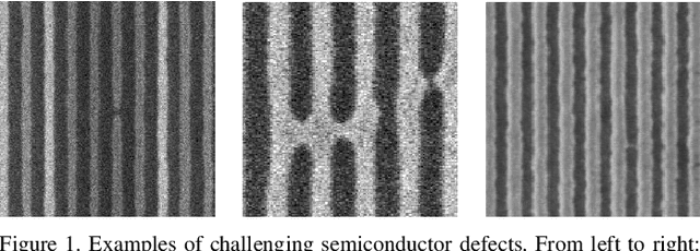
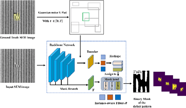
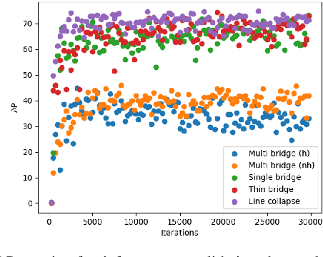
With continuous progression of Moore's Law, integrated circuit (IC) device complexity is also increasing. Scanning Electron Microscope (SEM) image based extensive defect inspection and accurate metrology extraction are two main challenges in advanced node (2 nm and beyond) technology. Deep learning (DL) algorithm based computer vision approaches gained popularity in semiconductor defect inspection over last few years. In this research work, a new semiconductor defect inspection framework "SEMI-DiffusionInst" is investigated and compared to previous frameworks. To the best of the authors' knowledge, this work is the first demonstration to accurately detect and precisely segment semiconductor defect patterns by using a diffusion model. Different feature extractor networks as backbones and data sampling strategies are investigated towards achieving a balanced trade-off between precision and computing efficiency. Our proposed approach outperforms previous work on overall mAP and performs comparatively better or as per for almost all defect classes (per class APs). The bounding box and segmentation mAPs achieved by the proposed SEMI-DiffusionInst model are improved by 3.83% and 2.10%,respectively. Among individual defect types, precision on line collapse and thin bridge defects are improved approximately 15% on detection task for both defect types. It has also been shown that by tuning inference hyperparameters, inference time can be improved significantly without compromising model precision. Finally, certain limitations and future work strategy to overcome them are discussed.
 Add to Chrome
 Add to Firefox
 Add to Edge