Shinjiro Umezu
Plant Doctor: A hybrid machine learning and image segmentation software to quantify plant damage in video footage
Jul 03, 2024Abstract:Artificial intelligence has significantly advanced the automation of diagnostic processes, benefiting various fields including agriculture. This study introduces an AI-based system for the automatic diagnosis of urban street plants using video footage obtained with accessible camera devices. The system aims to monitor plant health on a day-to-day basis, aiding in the control of disease spreading in urban areas. By combining two machine vision algorithms, YOLOv8 and DeepSORT, the system efficiently identifies and tracks individual leaves, extracting the optimal images for health analysis. YOLOv8, chosen for its speed and computational efficiency, locates leaves, while DeepSORT ensures robust tracking in complex environments. For detailed health assessment, DeepLabV3Plus, a convolutional neural network, is employed to segment and quantify leaf damage caused by bacteria, pests, and fungi. The hybrid system, named Plant Doctor, has been trained and validated using a diverse dataset including footage from Tokyo urban plants. The results demonstrate the robustness and accuracy of the system in diagnosing leaf damage, with potential applications in large scale urban flora illness monitoring. This approach provides a non-invasive, efficient, and scalable solution for urban tree health management, supporting sustainable urban ecosystems.
3D Programming of Patterned Heterogeneous Interface for 4D Smart Robotics
Dec 22, 2023Abstract:Shape memory structures are playing an important role in many cutting-edge intelligent fields. However, the existing technologies can only realize 4D printing of a single polymer or metal, which limits practical applications. Here, we report a construction strategy for TSMP/M heterointerface, which uses Pd2+-containing shape memory polymer (AP-SMR) to induce electroless plating reaction and relies on molecular dynamics, which has both shape memory properties and metal activity and information processing power. Through multi-material DLP 3D printing technology, the interface can be 3D selectively programmed on functional substrate parts of arbitrary shapes to become 4D electronic smart devices (Robotics). Microscopically, this type of interface appears as a composite structure with a nanometer-micrometer interface height, which is composed of a pure substrate layer (smart materials), an intermediate layer (a composite structure in which metal particles are embedded in a polymer cross-linked network) and a pure metal layer. The structure programmed by TSMP/M heterointerface exhibits both SMA characteristics and metal properties, thus having more intelligent functions (electroactive, electrothermal deformation, electronically controlled denaturation) and higher performance (selectivity of shape memory structures can be realized control, remote control, inline control and low voltage control). This is expected to provide a more flexible manufacturing process as platform technology for designing, manufacturing and applying smart devices with new concepts, and promote the development of cutting-edge industries such as smart robots and smart electronics.
New metal-plastic hybrid additive manufacturing strategy: Fabrication of arbitrary metal-patterns on external and even internal surfaces of 3D plastic structures
Dec 22, 2021


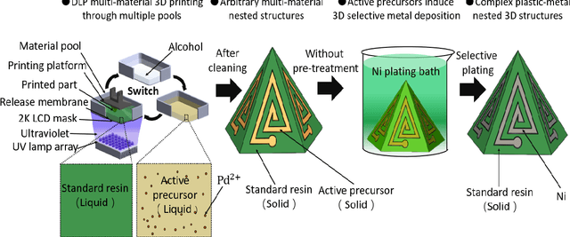
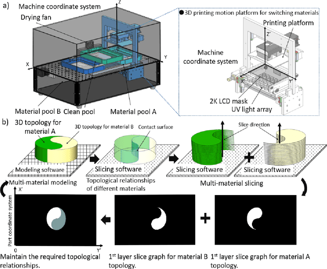
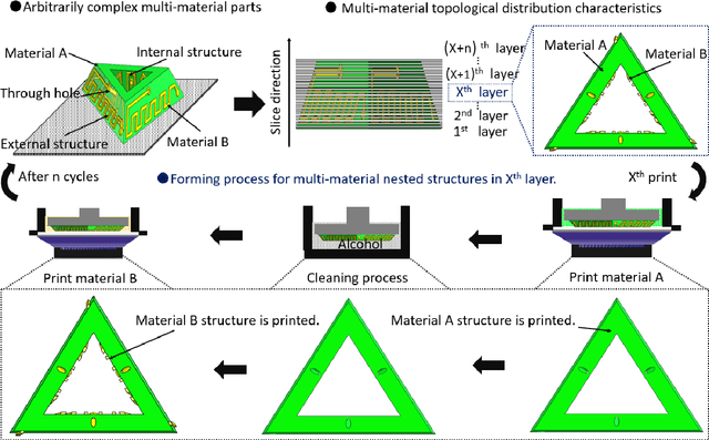
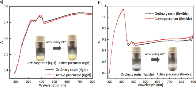
Abstract:Constructing precise micro-nano metal patterns on complex three-dimensional (3D) plastic parts allows the fabrication of functional devices for advanced applications. However, this patterning is currently expensive and requires complex processes with long manufacturing lead time. The present work demonstrates a process for the fabrication of micro-nano 3D metal-plastic composite structures with arbitrarily complex shapes. In this approach, a light-cured resin is modified to prepare an active precursor capable of allowing subsequent electroless plating (ELP). A multi-material digital light processing 3D printer was newly developed to enable the fabrication of parts containing regions made of either standard resin or active precursor resin nested within each other. Selective 3D ELP processing of such parts provided various metal-plastic composite parts having complicated hollow micro-nano structures with specific topological relationships on a size scale as small as 40 um. Using this technique, 3D metal topologies that cannot be manufactured by traditional methods are possible, and metal patterns can be produced inside plastic parts as a means of further miniaturizing electronic devices. The proposed method can also generate metal coatings exhibiting improved adhesion of metal to plastic substrate. Based on this technique, several sensors composed of different functional nonmetallic materials and specific metal patterns were designed and fabricated. The present results demonstrate the viability of the proposed method and suggest potential applications in the fields of smart 3D micro-nano electronics, 3D wearable devices, micro/nano-sensors, and health care.
 Add to Chrome
 Add to Firefox
 Add to Edge