Mark Kilgard
Generic Lithography Modeling with Dual-band Optics-Inspired Neural Networks
Mar 12, 2022


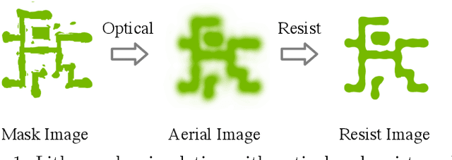
Abstract:Lithography simulation is a critical step in VLSI design and optimization for manufacturability. Existing solutions for highly accurate lithography simulation with rigorous models are computationally expensive and slow, even when equipped with various approximation techniques. Recently, machine learning has provided alternative solutions for lithography simulation tasks such as coarse-grained edge placement error regression and complete contour prediction. However, the impact of these learning-based methods has been limited due to restrictive usage scenarios or low simulation accuracy. To tackle these concerns, we introduce an dual-band optics-inspired neural network design that considers the optical physics underlying lithography. To the best of our knowledge, our approach yields the first published via/metal layer contour simulation at 1nm^2/pixel resolution with any tile size. Compared to previous machine learning based solutions, we demonstrate that our framework can be trained much faster and offers a significant improvement on efficiency and image quality with 20X smaller model size. We also achieve 85X simulation speedup over traditional lithography simulator with 1% accuracy loss.
 Add to Chrome
 Add to Firefox
 Add to Edge