Zehao Geng
Deep Learning Based Defect Detection for Solder Joints on Industrial X-Ray Circuit Board Images
Aug 06, 2020


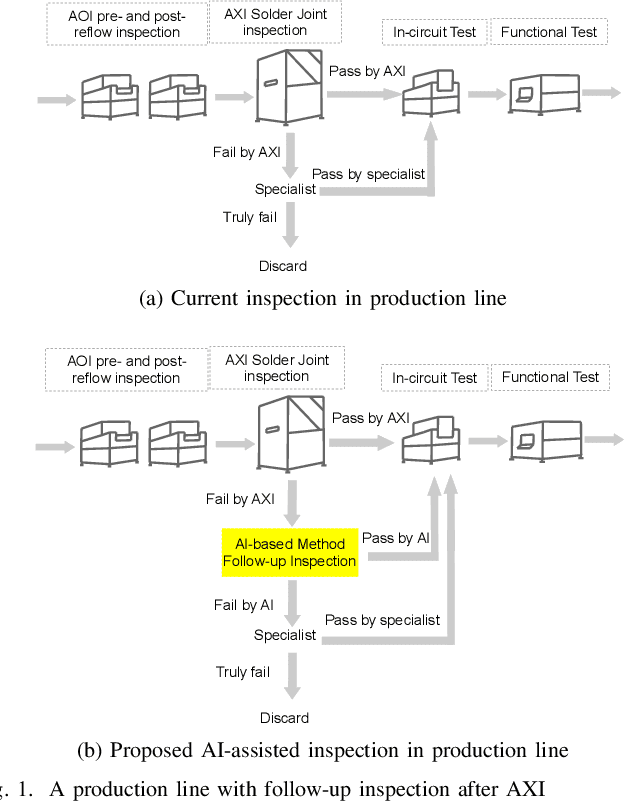
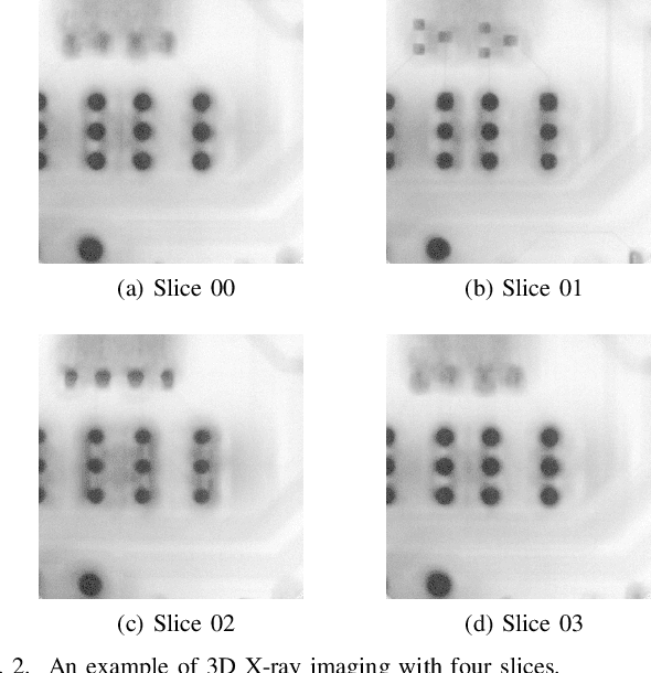
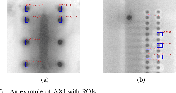
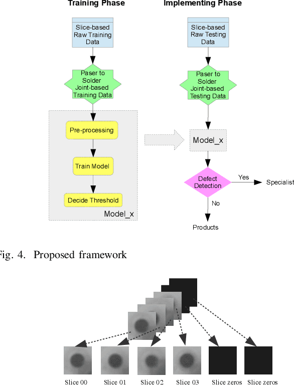
Abstract:Quality control is of vital importance during electronics production. As the methods of producing electronic circuits improve, there is an increasing chance of solder defects during assembling the printed circuit board (PCB). Many technologies have been incorporated for inspecting failed soldering, such as X-ray imaging, optical imaging, and thermal imaging. With some advanced algorithms, the new technologies are expected to control the production quality based on the digital images. However, current algorithms sometimes are not accurate enough to meet the quality control. Specialists are needed to do a follow-up checking. For automated X-ray inspection, joint of interest on the X-ray image is located by region of interest (ROI) and inspected by some algorithms. Some incorrect ROIs deteriorate the inspection algorithm. The high dimension of X-ray images and the varying sizes of image dimensions also challenge the inspection algorithms. On the other hand, recent advances on deep learning shed light on image-based tasks and are competitive to human levels. In this paper, deep learning is incorporated in X-ray imaging based quality control during PCB quality inspection. Two artificial intelligence (AI) based models are proposed and compared for joint defect detection. The noised ROI problem and the varying sizes of imaging dimension problem are addressed. The efficacy of the proposed methods are verified through experimenting on a real-world 3D X-ray dataset. By incorporating the proposed methods, specialist inspection workload is largely saved.
 Add to Chrome
 Add to Firefox
 Add to Edge