Sarma Vrudhula
HeteroSwitch: Characterizing and Taming System-Induced Data Heterogeneity in Federated Learning
Mar 07, 2024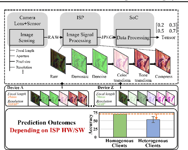


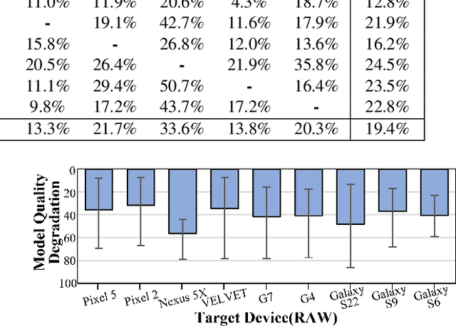
Abstract:Federated Learning (FL) is a practical approach to train deep learning models collaboratively across user-end devices, protecting user privacy by retaining raw data on-device. In FL, participating user-end devices are highly fragmented in terms of hardware and software configurations. Such fragmentation introduces a new type of data heterogeneity in FL, namely \textit{system-induced data heterogeneity}, as each device generates distinct data depending on its hardware and software configurations. In this paper, we first characterize the impact of system-induced data heterogeneity on FL model performance. We collect a dataset using heterogeneous devices with variations across vendors and performance tiers. By using this dataset, we demonstrate that \textit{system-induced data heterogeneity} negatively impacts accuracy, and deteriorates fairness and domain generalization problems in FL. To address these challenges, we propose HeteroSwitch, which adaptively adopts generalization techniques (i.e., ISP transformation and SWAD) depending on the level of bias caused by varying HW and SW configurations. In our evaluation with a realistic FL dataset (FLAIR), HeteroSwitch reduces the variance of averaged precision by 6.3\% across device types.
A Novel ASIC Design Flow using Weight-Tunable Binary Neurons as Standard Cells
Apr 17, 2022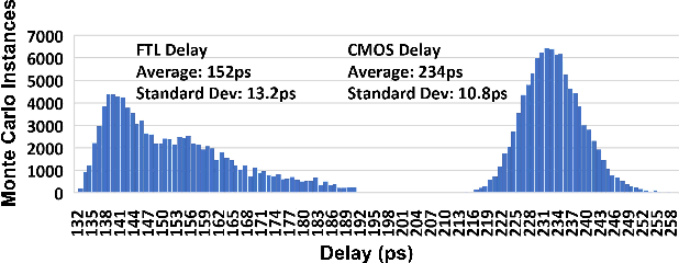
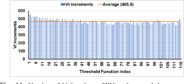
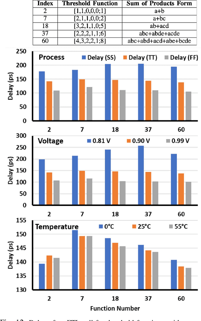
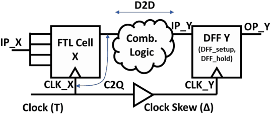
Abstract:In this paper, we describe a design of a mixed signal circuit for a binary neuron (a.k.a perceptron, threshold logic gate) and a methodology for automatically embedding such cells in ASICs. The binary neuron, referred to as an FTL (flash threshold logic) uses floating gate or flash transistors whose threshold voltages serve as a proxy for the weights of the neuron. Algorithms for mapping the weights to the flash transistor threshold voltages are presented. The threshold voltages are determined to maximize both the robustness of the cell and its speed. The performance, power, and area of a single FTL cell are shown to be significantly smaller (79.4%), consume less power (61.6%), and operate faster (40.3%) compared to conventional CMOS logic equivalents. Also included are the architecture and the algorithms to program the flash devices of an FTL. The FTL cells are implemented as standard cells, and are designed to allow commercial synthesis and P&R tools to automatically use them in synthesis of ASICs. Substantial reductions in area and power without sacrificing performance are demonstrated on several ASIC benchmarks by the automatic embedding of FTL cells. The paper also demonstrates how FTL cells can be used for fixing timing errors after fabrication.
A Configurable BNN ASIC using a Network of Programmable Threshold Logic Standard Cells
Apr 04, 2021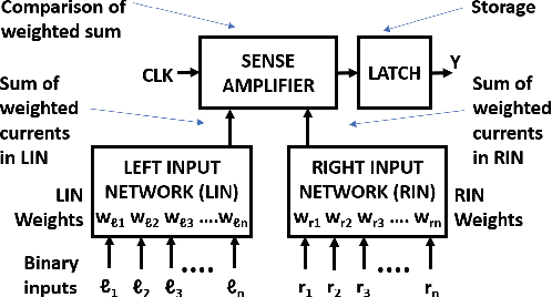
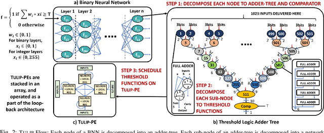
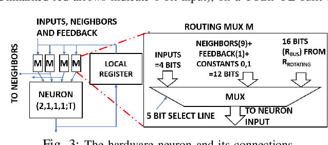
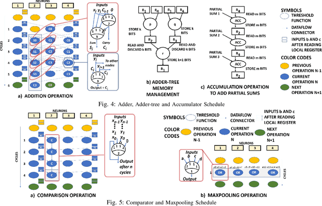
Abstract:This paper presents TULIP, a new architecture for a binary neural network (BNN) that uses an optimal schedule for executing the operations of an arbitrary BNN. It was constructed with the goal of maximizing energy efficiency per classification. At the top-level, TULIP consists of a collection of unique processing elements (TULIP-PEs) that are organized in a SIMD fashion. Each TULIP-PE consists of a small network of binary neurons, and a small amount of local memory per neuron. The unique aspect of the binary neuron is that it is implemented as a mixed-signal circuit that natively performs the inner-product and thresholding operation of an artificial binary neuron. Moreover, the binary neuron, which is implemented as a single CMOS standard cell, is reconfigurable, and with a change in a single parameter, can implement all standard operations involved in a BNN. We present novel algorithms for mapping arbitrary nodes of a BNN onto the TULIP-PEs. TULIP was implemented as an ASIC in TSMC 40nm-LP technology. To provide a fair comparison, a recently reported BNN that employs a conventional MAC-based arithmetic processor was also implemented in the same technology. The results show that TULIP is consistently 3X more energy-efficient than the conventional design, without any penalty in performance, area, or accuracy.
Enabling Incremental Knowledge Transfer for Object Detection at the Edge
Apr 13, 2020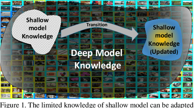
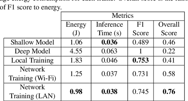
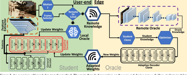
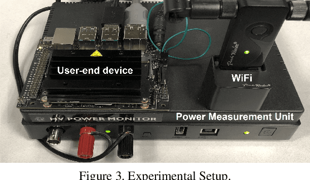
Abstract:Object detection using deep neural networks (DNNs) involves a huge amount of computation which impedes its implementation on resource/energy-limited user-end devices. The reason for the success of DNNs is due to having knowledge over all different domains of observed environments. However, we need a limited knowledge of the observed environment at inference time which can be learned using a shallow neural network (SHNN). In this paper, a system-level design is proposed to improve the energy consumption of object detection on the user-end device. An SHNN is deployed on the user-end device to detect objects in the observing environment. Also, a knowledge transfer mechanism is implemented to update the SHNN model using the DNN knowledge when there is a change in the object domain. DNN knowledge can be obtained from a powerful edge device connected to the user-end device through LAN or Wi-Fi. Experiments demonstrate that the energy consumption of the user-end device and the inference time can be improved by 78% and 40% compared with running the deep model on the user-end device.
ELSA: A Throughput-Optimized Design of an LSTM Accelerator for Energy-Constrained Devices
Oct 19, 2019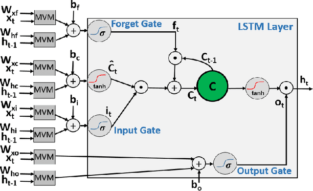

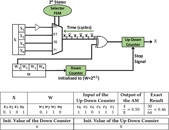

Abstract:The next significant step in the evolution and proliferation of artificial intelligence technology will be the integration of neural network (NN) models within embedded and mobile systems. This calls for the design of compact, energy efficient NN models in silicon. In this paper, we present a scalable ASIC design of an LSTM accelerator named ELSA, that is suitable for energy-constrained devices. It includes several architectural innovations to achieve small area and high energy efficiency. To reduce the area and power consumption of the overall design, the compute-intensive units of ELSA employ approximate multiplications and still achieve high performance and accuracy. The performance is further improved through efficient synchronization of the elastic pipeline stages to maximize the utilization. The paper also includes a performance model of ELSA, as a function of the hidden nodes and time steps, permitting its use for the evaluation of any LSTM application. ELSA was implemented in RTL and was synthesized and placed and routed in 65nm technology. Its functionality is demonstrated for language modeling-a common application of LSTM. ELSA is compared against a baseline implementation of an LSTM accelerator with standard functional units and without any of the architectural innovations of ELSA. The paper demonstrates that ELSA can achieve significant improvements in power, area and energy-efficiency when compared to the baseline design and several ASIC implementations reported in the literature, making it suitable for use in embedded systems and real-time applications.
 Add to Chrome
 Add to Firefox
 Add to Edge