Mehdi Habibi
An early shutdown circuit for power reduction in high-precision dynamic comparators
Oct 05, 2021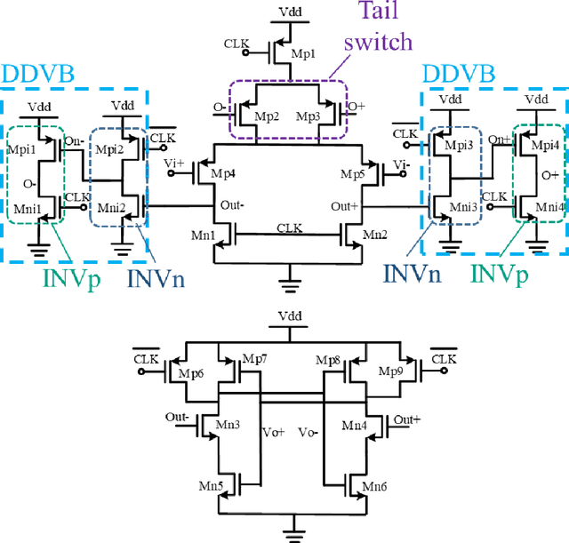

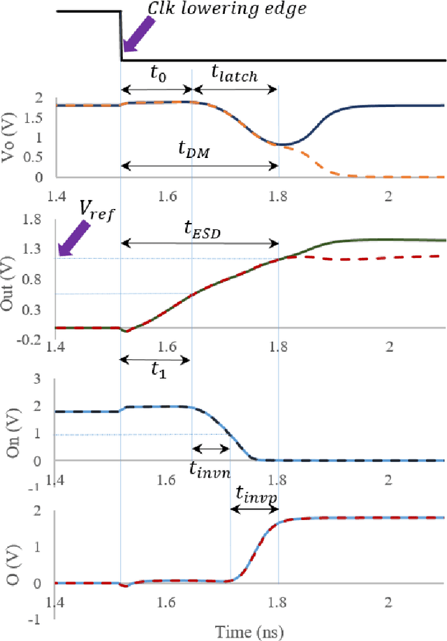
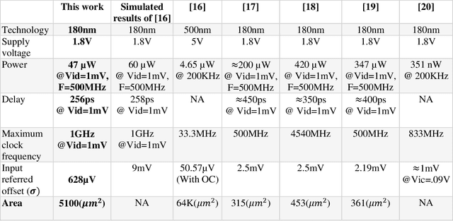
Abstract:Dynamic comparators are an essential part of low-power analog to digital converters (ADCs) and are referred to as one of the most important building blocks in mixed mode circuits. The power consumption and accuracy of dynamic comparators directly affects the overall power consumption and effective number of bits of the ADC. In this paper, an early shutdown approach is proposed to deactivate the first stage preamplifier at the suitable time. Furthermore, a time domain offset cancellation technique is incorporated to reduce offset effects. With the proposed method power consumption can be reduced in low power high precision dynamic comparators. The proposed method has been simulated in a standard 0.18{\mu}m CMOS technology and the results confirm its effectiveness. The proposed circuit has the ability of reducing the power consumption by 21.7% in the worst case, while having little effect on the speed and accuracy in comparison with the conventional methods. The proposed comparator consumes only 47{\mu}W while operating at 500MHz. Furthermore, Monte Carlo evaluations showed that the standard deviation of the residual input referred offset was 620{\mu}V.
CNFET-based design of efficient ternary half adder and 1-trit multiplier circuits using dynamic logic
Oct 05, 2021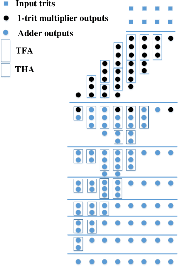


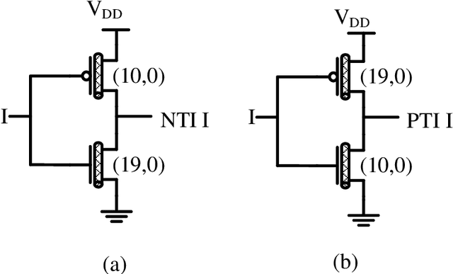
Abstract:This paper presents a ternary half adder and a 1-trit multiplier using carbon nanotube transistors. The proposed circuits are designed using pass transistor logic and dynamic logic. Ternary logic uses less connections than binary logic, and less voltage changes are required for the same amount of data transmission. Carbon nanotube transistors have advantages over MOSFETs, such as the same mobility for electrons and holes, the ability to adjust the threshold voltage by changing the nanotube diameter, and less leakage power. The proposed half adder has lower power consumption, delay, and fewer transistors compared to recent ternary half adders that use similar design methods. The proposed 1-trit multiplier also has a lower delay than other designs. Moreover, these advantages are achieved over a wide supply voltage range, operating temperatures, and output loads. The design is also more robust to process variations than the nearest design in terms of PDP.
A signed pulse-train based image processor-array for parallel kernel convolution in vision sensors
Oct 05, 2021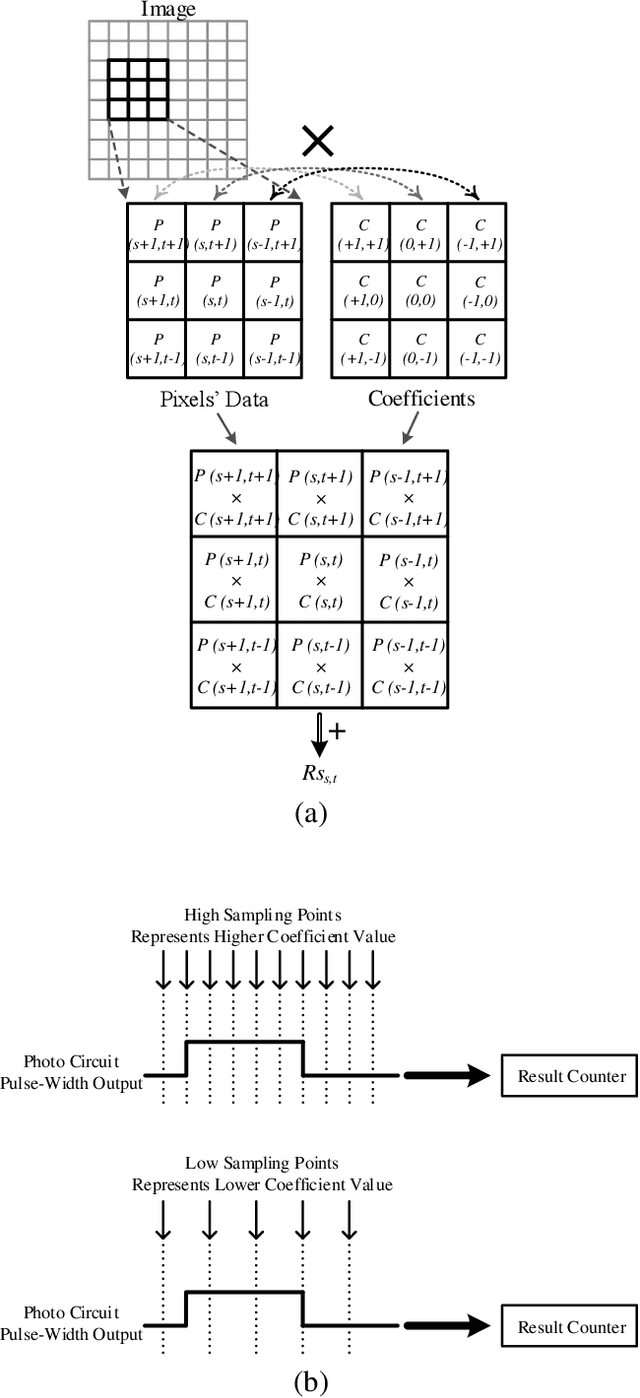
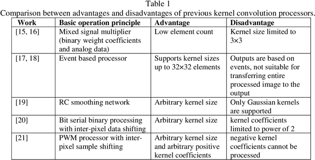
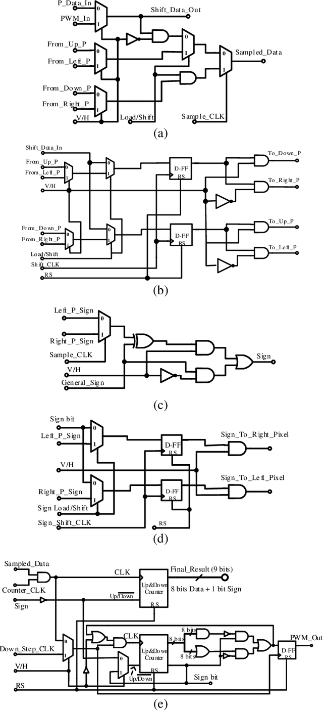
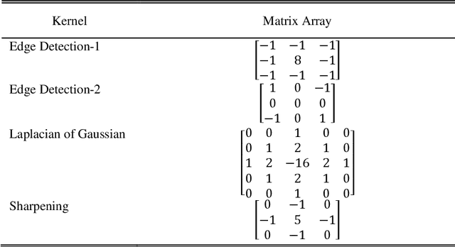
Abstract:Purpose- High speed image processing is a challenging task for real-time applications such as product quality control of manufacturing lines. Smart image sensors use an array of in-pixel processors to facilitate high-speed real-time image processing. These sensors are usually used to perform the initial low-level bulk image filtering and enhancement. Design- In this paper, using pulse-width modulated signals and regular nearest neighbor interconnections, a convolution image processor is presented. The presented processor is not only capable of processing arbitrary size kernels, but the kernel coefficients can be any arbitrary positive or negative floating number. Findings- The performance of the proposed architecture is evaluated on a FPGA platform. The peak signal-to-noise ratio (PSNR) metric is used to measure the computation error for different images, filters, and illuminations. Finally, the power consumption of the circuit in different operation conditions is presented. Originality/Value- The presented processor array can be used for high speed kernel convolution image processing tasks including arbitrary size edge detection and sharpening functions which require negative and fractional kernel values.
Nanopore-Based DNA Sequencing Sensors and CMOS Readout Approaches
Oct 05, 2021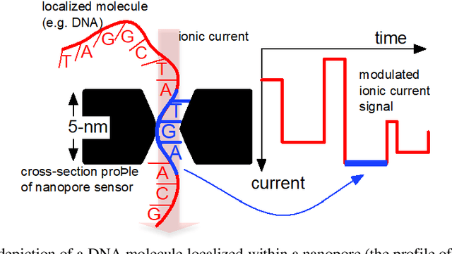
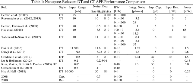
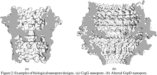

Abstract:Purpose Nanopore-based molecular sensing and measurement, specifically Deoxyribonucleic acid (DNA) sequencing, is advancing at a fast pace. Some embodiments have matured from coarse particle counters to enabling full human genome assembly. This evolution has been powered not only by improvements in the sensors themselves, but also in the assisting microelectronic Complementary Metal Oxide Semiconductor (CMOS) readout circuitry closely interfaced to them. In this light, this paper reviews established and emerging nanopore-based sensing modalities considered for DNA sequencing and CMOS microelectronic methods currently being used. Design/methodology/approach Readout and amplifier circuits which are potentially appropriate for conditioning and conversion of nanopore signals for downstream processing are studied. Furthermore, arrayed CMOS readout implementations are focused on and the relevant status of the nanopore sensor technology is reviewed as well. Findings Ion channel nanopore devices have properties unique compared with other electrochemical cells. Currently biological nanopores are the only variants reported which can be used for actual DNA sequencing. The translocation rate of DNA through such pores, the current range at which these cells operate on and the cell capacitance effect, all impose the necessity of using low noise circuits in the process of signal detection. The requirement of using in-pixel low noise circuits in turn tends to impose challenges in the implementation of large size arrays. Originality/value The study presents an overview on the readout circuits used for signal acquisition in electrochemical cell arrays and investigates the specific requirements necessary for implementation of nanopore type electrochemical cell amplifiers and their associated readout electronics.
A 0.4 V, 19 pW Subthreshold Voltage Reference Generator Using Separate Line Sensitivity and Temperature Coefficient Correction Stages
Oct 05, 2021

Abstract:Sensor nodes and IoT systems require blocks that not only consume low power but also have good accuracy. Voltage reference generators are also considered important building blocks in sensor interface circuits. This paper presents a solution to increase the accuracy of low power subthreshold voltage generators by lowering the circuit sensitivity to temperature and supply voltage variations. The enhancement is achieved by using two separate stages for temperature coefficient (TC) and line sensitivity (LS) correction. A 0.18 {\mu}m standard CMOS process has been used for the proposed structure. The effects of parameter variations in the fabrication process are investigated using post-layout simulation and Monte Carlo analysis. In the supply voltage of 0.4 V to 2 V, an LS of 143.8 ppm/V is obtained. In typical corner conditions, the achieved TC is 7.45 ppm/{\circ}C over the temperature range of 0{\circ}C to 80{\circ}C. Due to process changes, and mainly affected by threshold voltage variations, the average TC can change to 39.2 ppm/{\circ}C. The minimum power consumption at 0{\circ}C and at a supply voltage of 0.4 V is 3.25 pW while the power consumption increases to 2.84 nW in 80{\circ}C and at the maximum supply voltage of 2 V.
 Add to Chrome
 Add to Firefox
 Add to Edge