Yueguang Zhang
On-chip Real-time Hyperspectral Imager with Full CMOS Resolution Enabled by Massively Parallel Neural Network
Apr 15, 2024
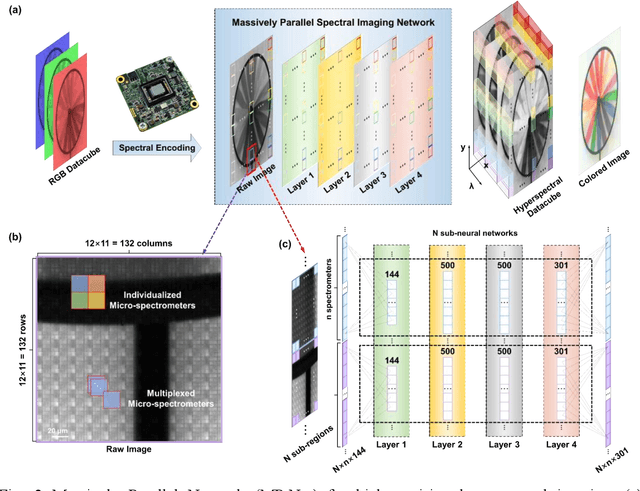
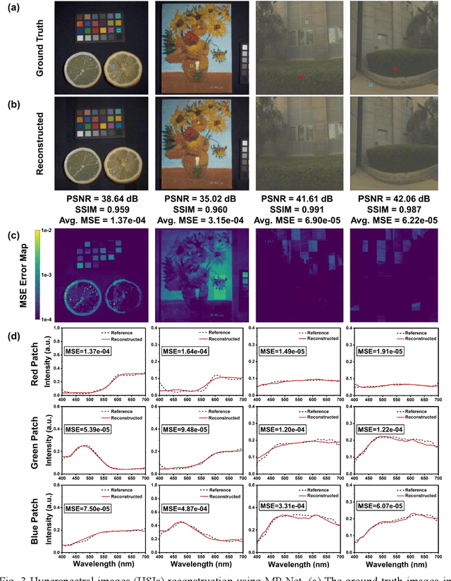
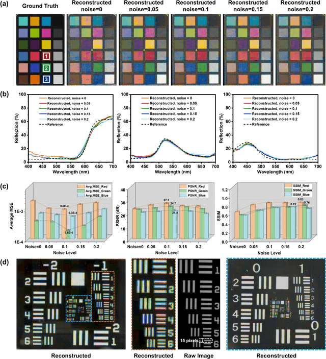
Abstract:Traditional spectral imaging methods are constrained by the time-consuming scanning process, limiting the application in dynamic scenarios. One-shot spectral imaging based on reconstruction has been a hot research topic recently and the primary challenges still lie in both efficient fabrication techniques suitable for mass production and the high-speed, high-accuracy reconstruction algorithm for real-time spectral imaging. In this study, we introduce an innovative on-chip real-time hyperspectral imager that leverages nanophotonic film spectral encoders and a Massively Parallel Network (MP-Net), featuring a 4 * 4 array of compact, all-dielectric film units for the micro-spectrometers. Each curved nanophotonic film unit uniquely modulates incident light across the underlying 3 * 3 CMOS image sensor (CIS) pixels, enabling a high spatial resolution equivalent to the full CMOS resolution. The implementation of MP-Net, specially designed to address variability in transmittance and manufacturing errors such as misalignment and non-uniformities in thin film deposition, can greatly increase the structural tolerance of the device and reduce the preparation requirement, further simplifying the manufacturing process. Tested in varied environments on both static and moving objects, the real-time hyperspectral imager demonstrates the robustness and high-fidelity spatial-spectral data capabilities across diverse scenarios. This on-chip hyperspectral imager represents a significant advancement in real-time, high-resolution spectral imaging, offering a versatile solution for applications ranging from environmental monitoring, remote sensing to consumer electronics.
1-bit Quantized On-chip Hybrid Diffraction Neural Network Enabled by Authentic All-optical Fully-connected Architecture
Apr 11, 2024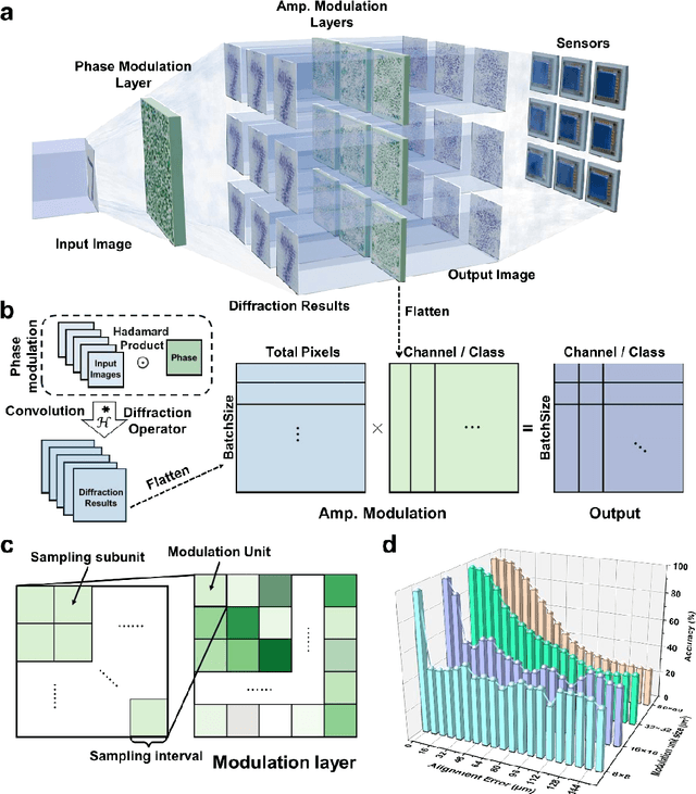
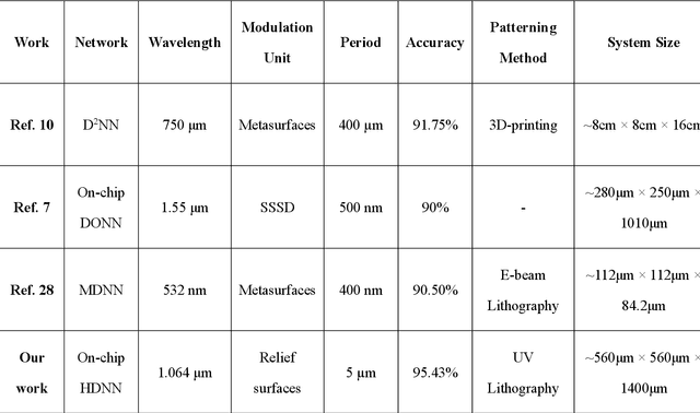

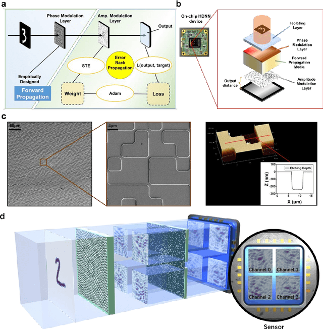
Abstract:Optical Diffraction Neural Networks (DNNs), a subset of Optical Neural Networks (ONNs), show promise in mirroring the prowess of electronic networks. This study introduces the Hybrid Diffraction Neural Network (HDNN), a novel architecture that incorporates matrix multiplication into DNNs, synergizing the benefits of conventional ONNs with those of DNNs to surmount the modulation limitations inherent in optical diffraction neural networks. Utilizing a singular phase modulation layer and an amplitude modulation layer, the trained neural network demonstrated remarkable accuracies of 96.39% and 89% in digit recognition tasks in simulation and experiment, respectively. Additionally, we develop the Binning Design (BD) method, which effectively mitigates the constraints imposed by sampling intervals on diffraction units, substantially streamlining experimental procedures. Furthermore, we propose an on-chip HDNN that not only employs a beam-splitting phase modulation layer for enhanced integration level but also significantly relaxes device fabrication requirements, replacing metasurfaces with relief surfaces designed by 1-bit quantization. Besides, we conceptualized an all-optical HDNN-assisted lesion detection network, achieving detection outcomes that were 100% aligned with simulation predictions. This work not only advances the performance of DNNs but also streamlines the path towards industrial optical neural network production.
 Add to Chrome
 Add to Firefox
 Add to Edge