Maike Lorena Stern
Playing Ping Pong with Light: Directional Emission of White Light
Nov 30, 2021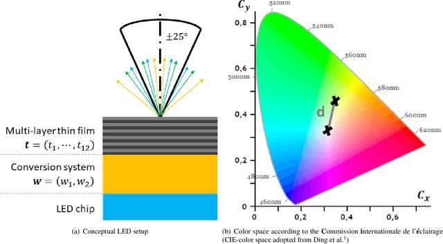

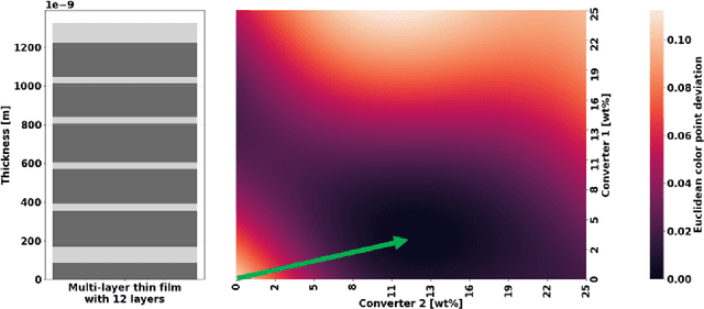

Abstract:Over the last decades, light-emitting diodes (LED) have replaced common light bulbs in almost every application, from flashlights in smartphones to automotive headlights. Illuminating nightly streets requires LEDs to emit a light spectrum that is perceived as pure white by the human eye. The power associated with such a white light spectrum is not only distributed over the contributing wavelengths but also over the angles of vision. For many applications, the usable light rays are required to exit the LED in forward direction, namely under small angles to the perpendicular. In this work, we demonstrate that a specifically designed multi-layer thin film on top of a white LED increases the power of pure white light emitted in forward direction. Therefore, the deduced multi-objective optimization problem is reformulated via a real-valued physics-guided objective function that represents the hierarchical structure of our engineering problem. Variants of Bayesian optimization are employed to maximize this non-deterministic objective function based on ray tracing simulations. Eventually, the investigation of optical properties of suitable multi-layer thin films allowed to identify the mechanism behind the increased directionality of white light: angle and wavelength selective filtering causes the multi-layer thin film to play ping pong with rays of light.
Rethinking Fully Convolutional Networks for the Analysis of Photoluminescence Wafer Images
Mar 01, 2020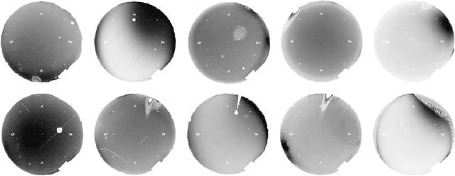
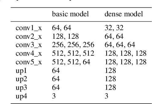
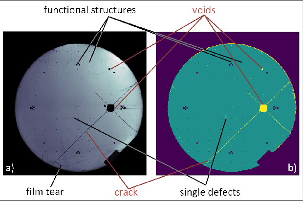
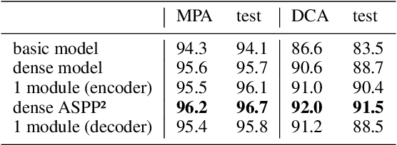
Abstract:The manufacturing of light-emitting diodes is a complex semiconductor-manufacturing process, interspersed with different measurements. Among the employed measurements, photoluminescence imaging has several advantages, namely being a non-destructive, fast and thus cost-effective measurement. On a photoluminescence measurement image of an LED wafer, every pixel corresponds to an LED chip's brightness after photo-excitation, revealing chip performance information. However, generating a chip-fine defect map of the LED wafer, based on photoluminescence images, proves challenging for multiple reasons: on the one hand, the measured brightness values vary from image to image, in addition to local spots of differing brightness. On the other hand, certain defect structures may assume multiple shapes, sizes and brightness gradients, where salient brightness values may correspond to defective LED chips, measurement artefacts or non-defective structures. In this work, we revisit the creation of chip-fine defect maps using fully convolutional networks and show that the problem of segmenting objects at multiple scales can be improved by the incorporation of densely connected convolutional blocks and atrous spatial pyramid pooling modules. We also share implementation details and our experiences with training networks with small datasets of measurement images. The proposed architecture significantly improves the segmentation accuracy of highly variable defect structures over our previous version.
Fully Convolutional Networks for Chip-wise Defect Detection Employing Photoluminescence Images
Oct 06, 2019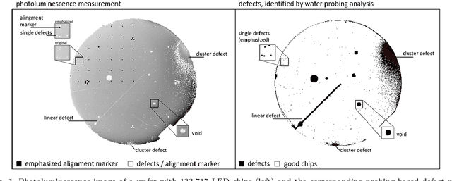
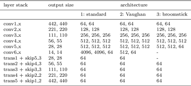
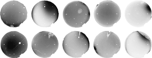

Abstract:Efficient quality control is inevitable in the manufacturing of light-emitting diodes (LEDs). Because defective LED chips may be traced back to different causes, a time and cost-intensive electrical and optical contact measurement is employed. Fast photoluminescence measurements, on the other hand, are commonly used to detect wafer separation damages but also hold the potential to enable an efficient detection of all kinds of defective LED chips. On a photoluminescence image, every pixel corresponds to an LED chip's brightness after photoexcitation, revealing performance information. But due to unevenly distributed brightness values and varying defect patterns, photoluminescence images are not yet employed for a comprehensive defect detection. In this work, we show that fully convolutional networks can be used for chip-wise defect detection, trained on a small data-set of photoluminescence images. Pixel-wise labels allow us to classify each and every chip as defective or not. Being measurement-based, labels are easy to procure and our experiments show that existing discrepancies between training images and labels do not hinder network training. Using weighted loss calculation, we were able to equalize our highly unbalanced class categories. Due to the consistent use of skip connections and residual shortcuts, our network is able to predict a variety of structures, from extensive defect clusters up to single defective LED chips.
 Add to Chrome
 Add to Firefox
 Add to Edge