Rethinking Fully Convolutional Networks for the Analysis of Photoluminescence Wafer Images
Paper and Code
Mar 01, 2020


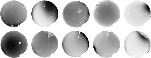
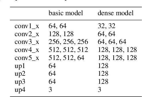
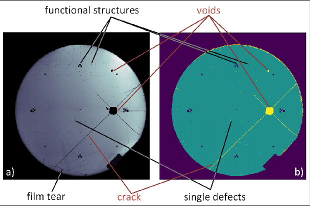
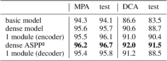
The manufacturing of light-emitting diodes is a complex semiconductor-manufacturing process, interspersed with different measurements. Among the employed measurements, photoluminescence imaging has several advantages, namely being a non-destructive, fast and thus cost-effective measurement. On a photoluminescence measurement image of an LED wafer, every pixel corresponds to an LED chip's brightness after photo-excitation, revealing chip performance information. However, generating a chip-fine defect map of the LED wafer, based on photoluminescence images, proves challenging for multiple reasons: on the one hand, the measured brightness values vary from image to image, in addition to local spots of differing brightness. On the other hand, certain defect structures may assume multiple shapes, sizes and brightness gradients, where salient brightness values may correspond to defective LED chips, measurement artefacts or non-defective structures. In this work, we revisit the creation of chip-fine defect maps using fully convolutional networks and show that the problem of segmenting objects at multiple scales can be improved by the incorporation of densely connected convolutional blocks and atrous spatial pyramid pooling modules. We also share implementation details and our experiences with training networks with small datasets of measurement images. The proposed architecture significantly improves the segmentation accuracy of highly variable defect structures over our previous version.
 Add to Chrome
 Add to Firefox
 Add to Edge