Data Efficient Lithography Modeling with Transfer Learning and Active Data Selection
Paper and Code
Jun 27, 2018


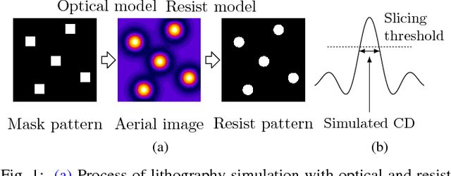
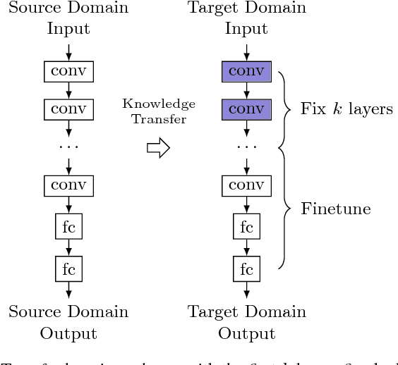
Lithography simulation is one of the key steps in physical verification, enabled by the substantial optical and resist models. A resist model bridges the aerial image simulation to printed patterns. While the effectiveness of learning-based solutions for resist modeling has been demonstrated, they are considerably data-demanding. Meanwhile, a set of manufactured data for a specific lithography configuration is only valid for the training of one single model, indicating low data efficiency. Due to the complexity of the manufacturing process, obtaining enough data for acceptable accuracy becomes very expensive in terms of both time and cost, especially during the evolution of technology generations when the design space is intensively explored. In this work, we propose a new resist modeling framework for contact layers, utilizing existing data from old technology nodes and active selection of data in a target technology node, to reduce the amount of data required from the target lithography configuration. Our framework based on transfer learning and active learning techniques is effective within a competitive range of accuracy, i.e., 3-10X reduction on the amount of training data with comparable accuracy to the state-of-the-art learning approach.
 Add to Chrome
 Add to Firefox
 Add to Edge