Adaptive Defective Area Identification in Material Surface Using Active Transfer Learning-based Level Set Estimation
Paper and Code
Apr 03, 2023


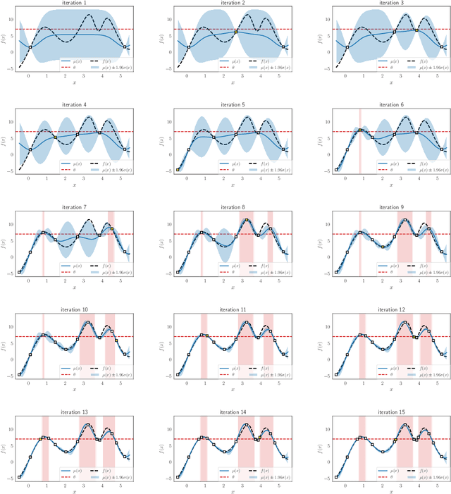
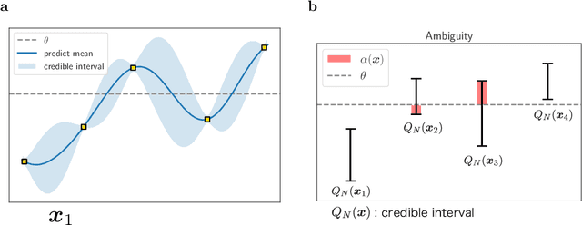
In material characterization, identifying defective areas on a material surface is fundamental. The conventional approach involves measuring the relevant physical properties point-by-point at the predetermined mesh grid points on the surface and determining the area at which the property does not reach the desired level. To identify defective areas more efficiently, we propose adaptive mapping methods in which measurement resources are used preferentially to detect the boundaries of defective areas. We interpret this problem as an active-learning (AL) of the level set estimation (LSE) problem. The goal of AL-based LSE is to determine the level set of the physical property function defined on the surface with as small number of measurements as possible. Furthermore, to handle the situations in which materials with similar specifications are repeatedly produced, we introduce a transfer learning approach so that the information of previously produced materials can be effectively utilized. As a proof-of-concept, we applied the proposed methods to the red-zone estimation problem of silicon wafers and demonstrated that we could identify the defective areas with significantly lower measurement costs than those of conventional methods.
 Add to Chrome
 Add to Firefox
 Add to Edge