Sparsity-Based Super Resolution for SEM Images
Paper and Code
Aug 29, 2017


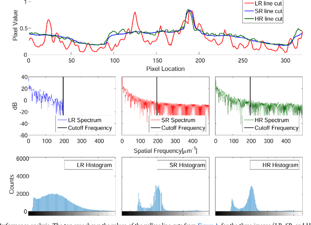
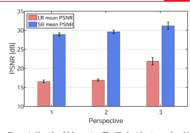
The scanning electron microscope (SEM) produces an image of a sample by scanning it with a focused beam of electrons. The electrons interact with the atoms in the sample, which emit secondary electrons that contain information about the surface topography and composition. The sample is scanned by the electron beam point by point, until an image of the surface is formed. Since its invention in 1942, SEMs have become paramount in the discovery and understanding of the nanometer world, and today it is extensively used for both research and in industry. In principle, SEMs can achieve resolution better than one nanometer. However, for many applications, working at sub-nanometer resolution implies an exceedingly large number of scanning points. For exactly this reason, the SEM diagnostics of microelectronic chips is performed either at high resolution (HR) over a small area or at low resolution (LR) while capturing a larger portion of the chip. Here, we employ sparse coding and dictionary learning to algorithmically enhance LR SEM images of microelectronic chips up to the level of the HR images acquired by slow SEM scans, while considerably reducing the noise. Our methodology consists of two steps: an offline stage of learning a joint dictionary from a sequence of LR and HR images of the same region in the chip, followed by a fast-online super-resolution step where the resolution of a new LR image is enhanced. We provide several examples with typical chips used in the microelectronics industry, as well as a statistical study on arbitrary images with characteristic structural features. Conceptually, our method works well when the images have similar characteristics. This work demonstrates that employing sparsity concepts can greatly improve the performance of SEM, thereby considerably increasing the scanning throughput without compromising on analysis quality and resolution.
 Add to Chrome
 Add to Firefox
 Add to Edge