SEMU-Net: A Segmentation-based Corrector for Fabrication Process Variations of Nanophotonics with Microscopic Images
Paper and Code
Nov 25, 2024


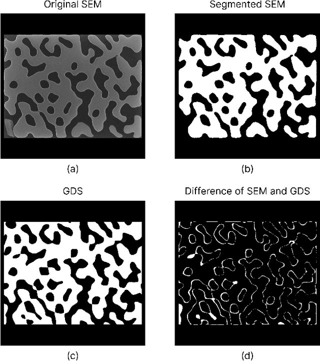
Integrated silicon photonic devices, which manipulate light to transmit and process information on a silicon-on-insulator chip, are highly sensitive to structural variations. Minor deviations during nanofabrication-the precise process of building structures at the nanometer scale-such as over- or under-etching, corner rounding, and unintended defects, can significantly impact performance. To address these challenges, we introduce SEMU-Net, a comprehensive set of methods that automatically segments scanning electron microscope images (SEM) and uses them to train two deep neural network models based on U-Net and its variants. The predictor model anticipates fabrication-induced variations, while the corrector model adjusts the design to address these issues, ensuring that the final fabricated structures closely align with the intended specifications. Experimental results show that the segmentation U-Net reaches an average IoU score of 99.30%, while the corrector attention U-Net in a tandem architecture achieves an average IoU score of 98.67%.
 Add to Chrome
 Add to Firefox
 Add to Edge