Design-Technology Co-Optimization for NVM-based Neuromorphic Processing Elements
Paper and Code
Mar 10, 2022


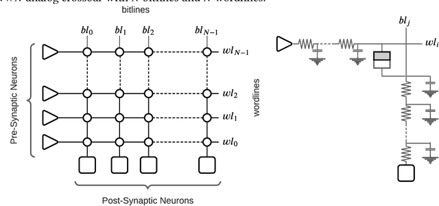
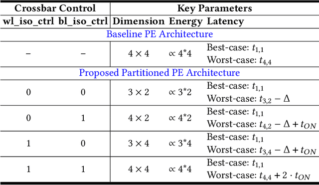
Neuromorphic hardware platforms can significantly lower the energy overhead of a machine learning inference task. We present a design-technology tradeoff analysis to implement such inference tasks on the processing elements (PEs) of a Non- Volatile Memory (NVM)-based neuromorphic hardware. Through detailed circuit-level simulations at scaled process technology nodes, we show the negative impact of technology scaling on the information-processing latency, which impacts the quality-of-service (QoS) of an embedded ML system. At a finer granularity, the latency inside a PE depends on 1) the delay introduced by parasitic components on its current paths, and 2) the varying delay to sense different resistance states of its NVM cells. Based on these two observations, we make the following three contributions. First, on the technology front, we propose an optimization scheme where the NVM resistance state that takes the longest time to sense is set on current paths having the least delay, and vice versa, reducing the average PE latency, which improves the QoS. Second, on the architecture front, we introduce isolation transistors within each PE to partition it into regions that can be individually power-gated, reducing both latency and energy. Finally, on the system-software front, we propose a mechanism to leverage the proposed technological and architectural enhancements when implementing a machine-learning inference task on neuromorphic PEs of the hardware. Evaluations with a recent neuromorphic hardware architecture show that our proposed design-technology co-optimization approach improves both performance and energy efficiency of machine-learning inference tasks without incurring high cost-per-bit.
 Add to Chrome
 Add to Firefox
 Add to Edge