Omid Hemmatyar
Knowledge Discovery In Nanophotonics Using Geometric Deep Learning
Sep 16, 2019


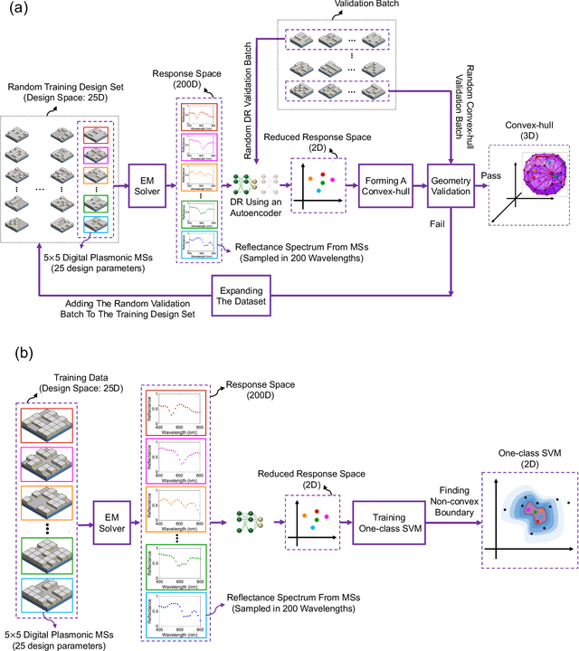
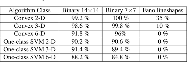
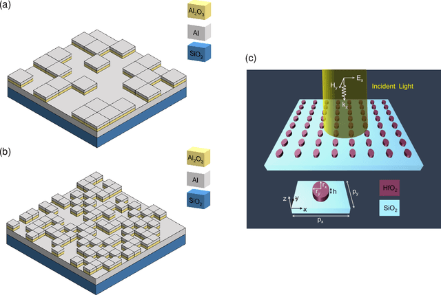
Abstract:We present here a new approach for using the intelligence aspects of artificial intelligence for knowledge discovery rather than device optimization in electromagnetic (EM) nanostructures. This approach uses training data obtained through full-wave EM simulations of a series of nanostructures to train geometric deep learning algorithms to assess the range of feasible responses as well as the feasibility of a desired response from a class of EM nanostructures. To facilitate the knowledge discovery and reduce the computation complexity, our approach combines the dimensionality reduction technique (using an autoencoder) with convex-hull and one-class support-vector-machine (SVM) algorithms to find the range of the feasible responses in the latent (or the reduced) response space of the EM nanostructure. We show that by using a small set of training instances (compared to all possible structures), our approach can provide better than 95% accuracy in assessing the feasibility of a given response. More importantly, the one-class SVM algorithm can be trained to provide the degree of feasibility (or unfeasibility) of a response from a given nanostructure. This important information can be used to modify the initial structure to an alternative one that can enable an initially unfeasible response. To show the applicability of our approach, we apply it to two important classes of binary metasurfaces (MSs), formed by array of plasmonic nanostructures, and periodic MSs formed by an array of dielectric nanopillars. In addition to theoretical results, we show the experimental results obtained by fabricating several MSs of the second class. Our theoretical and experimental results confirm the unique features of this approach for knowledge discovery in EM nanostructures.
Deep Learning Reveals Underlying Physics of Light-matter Interactions in Nanophotonic Devices
May 07, 2019


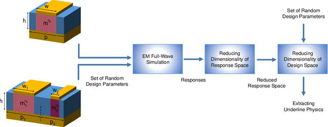
Abstract:In this paper, we present a deep learning-based (DL-based) algorithm, as a purely mathematical platform, for providing intuitive understanding of the properties of electromagnetic (EM) wave-matter interaction in nanostructures. This approach is based on using the dimensionality reduction (DR) technique to significantly reduce the dimensionality of a generic EM wave-matter interaction problem without imposing significant error. Such an approach implicitly provides useful information about the role of different features (or design parameters such as geometry) of the nanostructure in its response functionality. To demonstrate the practical capabilities of this DL-based technique, we apply it to a reconfigurable optical metadevice enabling dual-band and triple-band optical absorption in the telecommunication window. Combination of the proposed approach with existing commercialized full-wave simulation tools offers a powerful toolkit to extract basic mechanisms of wave-matter interaction in complex EM devices and facilitate the design and optimization of nanostructures for a large range of applications including imaging, spectroscopy, and signal processing. It is worth to mention that the demonstrated approach is general and can be used in a large range of problems as long as enough training data can be provided.
 Add to Chrome
 Add to Firefox
 Add to Edge