Deep Learning Reveals Underlying Physics of Light-matter Interactions in Nanophotonic Devices
Paper and Code
May 07, 2019


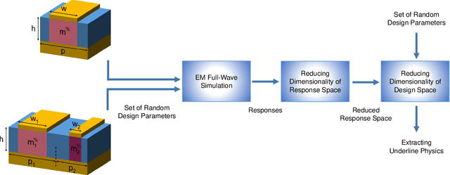
In this paper, we present a deep learning-based (DL-based) algorithm, as a purely mathematical platform, for providing intuitive understanding of the properties of electromagnetic (EM) wave-matter interaction in nanostructures. This approach is based on using the dimensionality reduction (DR) technique to significantly reduce the dimensionality of a generic EM wave-matter interaction problem without imposing significant error. Such an approach implicitly provides useful information about the role of different features (or design parameters such as geometry) of the nanostructure in its response functionality. To demonstrate the practical capabilities of this DL-based technique, we apply it to a reconfigurable optical metadevice enabling dual-band and triple-band optical absorption in the telecommunication window. Combination of the proposed approach with existing commercialized full-wave simulation tools offers a powerful toolkit to extract basic mechanisms of wave-matter interaction in complex EM devices and facilitate the design and optimization of nanostructures for a large range of applications including imaging, spectroscopy, and signal processing. It is worth to mention that the demonstrated approach is general and can be used in a large range of problems as long as enough training data can be provided.
 Add to Chrome
 Add to Firefox
 Add to Edge