Marilyne Sousa
Learning-based Defect Recognition for Quasi-Periodic Microscope Images
Jul 02, 2020


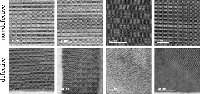
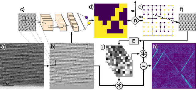
Abstract:The detailed control of crystalline material defects is a crucial process, as they affect properties of the material that may be detrimental or beneficial for the final performance of a device. Defect analysis on the sub-nanometer scale is enabled by high-resolution transmission electron microscopy (HRTEM), where the identification of defects is currently carried out based on human expertise. However, the process is tedious, highly time consuming and, in some cases, can yield to ambiguous results. Here we propose a semi-supervised machine learning method that assists in the detection of lattice defects from atomic resolution microscope images. It involves a convolutional neural network that classifies image patches as defective or non-defective, a graph-based heuristic that chooses one non-defective patch as a model, and finally an automatically generated convolutional filter bank, which highlights symmetry breaking such as stacking faults, twin defects and grain boundaries. Additionally, a variance filter is suggested to segment amorphous regions and beam defects. The algorithm is tested on III-V/Si crystalline materials and successfully evaluated against different metrics, showing promising results even for extremely small data sets. By combining the data-driven classification generality, robustness and speed of deep learning with the effectiveness of image filters in segmenting faulty symmetry arrangements, we provide a valuable open-source tool to the microscopist community that can streamline future HRTEM analyses of crystalline materials.
 Add to Chrome
 Add to Firefox
 Add to Edge