L. A. Camuñas-Mesa
A CMOL-Like Memristor-CMOS Neuromorphic Chip-Core Demonstrating Stochastic Binary STDP
Sep 13, 2022


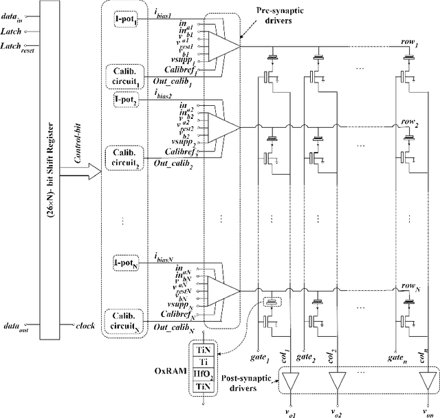
Abstract:The advent of nanoscale memristors raised hopes of being able to build CMOL (CMOS/nanowire/moLecular) type ultra-dense in-memory-computing circuit architectures. In CMOL, nanoscale memristors would be fabricated at the intersection of nanowires. The CMOL concept can be exploited in neuromorphic hardware by fabricating lower-density neurons on CMOS and placing massive analog synaptic connectivity with nanowire and nanoscale-memristor fabric post-fabricated on top. However, technical problems have hindered such developments for presently available reliable commercial monolithic CMOS-memristor technologies. On one hand, each memristor needs a MOS selector transistor in series to guarantee forming and programming operations in large arrays. This results in compound MOS-memristor synapses (called 1T1R) which are no longer synapses at the crossing of nanowires. On the other hand, memristors do not yet constitute highly reliable, stable analog memories for massive analog-weight synapses with gradual learning. Here we demonstrate a pseudo-CMOL monolithic chip core that circumvents the two technical problems mentioned above by (a) exploiting a CMOL-like geometrical chip layout technique to improve density despite the 1T1R limitation, and (b) exploiting a binary weight stochastic Spike-Timing-Dependent-Plasticity (STDP) learning rule that takes advantage of the more reliable binary memory capability of the memristors used. Experimental results are provided for a spiking neural network (SNN) CMOL-core with 64 input neurons, 64 output neurons, and 4096 1T1R synapses, fabricated in 130nm CMOS with 200nm-sized Ti/HfOx/TiN memristors on top. The CMOL-core uses query-driven event read-out, which allows for memristor variability insensitive computations.
Experimental Body-input Three-stage DC offset Calibration Scheme for Memristive Crossbar
Mar 03, 2021


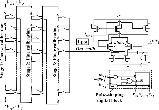
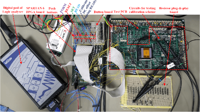
Abstract:Reading several ReRAMs simultaneously in a neuromorphic circuit increases power consumption and limits scalability. Applying small inference read pulses is a vain attempt when offset voltages of the read-out circuit are decisively more. This paper presents an experimental validation of a three-stage calibration scheme to calibrate the DC offset voltage across the rows of the memristive crossbar. The proposed method is based on biasing the body terminal of one of the differential pair MOSFETs of the buffer through a series of cascaded resistor banks arranged in three stages: coarse, fine and finer stages. The circuit is designed in a 130 nm CMOS technology, where the OxRAM-based binary memristors are built on top of it. A dedicated PCB and other auxiliary boards have been designed for testing the chip. Experimental results validate the presented approach, which is only limited by mismatch and electrical noise.
 Add to Chrome
 Add to Firefox
 Add to Edge