Machine-learning based methodologies for 3d x-ray measurement, characterization and optimization for buried structures in advanced ic packages
Paper and Code
Mar 08, 2021


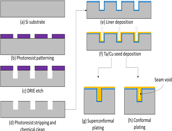
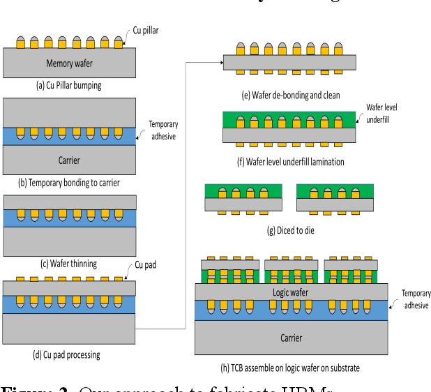
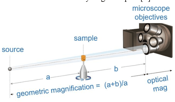
For over 40 years lithographic silicon scaling has driven circuit integration and performance improvement in the semiconductor industry. As silicon scaling slows down, the industry is increasingly dependent on IC package technologies to contribute to further circuit integration and performance improvements. This is a paradigm shift and requires the IC package industry to reduce the size and increase the density of internal interconnects on a scale which has never been done before. Traditional package characterization and process optimization relies on destructive techniques such as physical cross-sections and delayering to extract data from internal package features. These destructive techniques are not practical with today's advanced packages. In this paper we will demonstrate how data acquired non-destructively with a 3D X-ray microscope can be enhanced and optimized using machine learning, and can then be used to measure, characterize and optimize the design and production of buried interconnects in advanced IC packages. Test vehicles replicating 2.5D and HBM construction were designed and fabricated, and digital data was extracted from these test vehicles using 3D X-ray and machine learning techniques. The extracted digital data was used to characterize and optimize the design and production of the interconnects and demonstrates a superior alternative to destructive physical analysis. We report an mAP of 0.96 for 3D object detection, a dice score of 0.92 for 3D segmentation, and an average of 2.1um error for 3D metrology on the test dataset. This paper is the first part of a multi-part report.
 Add to Chrome
 Add to Firefox
 Add to Edge