Improving Automated Visual Fault Detection by Combining a Biologically Plausible Model of Visual Attention with Deep Learning
Paper and Code
Feb 13, 2021


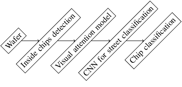
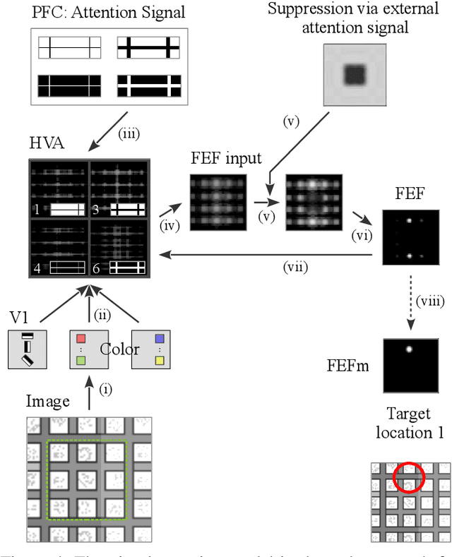
It is a long-term goal to transfer biological processing principles as well as the power of human recognition into machine vision and engineering systems. One of such principles is visual attention, a smart human concept which focuses processing on a part of a scene. In this contribution, we utilize attention to improve the automatic detection of defect patterns for wafers within the domain of semiconductor manufacturing. Previous works in the domain have often utilized classical machine learning approaches such as KNNs, SVMs, or MLPs, while a few have already used modern approaches like deep neural networks (DNNs). However, one problem in the domain is that the faults are often very small and have to be detected within a larger size of the chip or even the wafer. Therefore, small structures in the size of pixels have to be detected in a vast amount of image data. One interesting principle of the human brain for solving this problem is visual attention. Hence, we employ here a biologically plausible model of visual attention for automatic visual inspection. We propose a hybrid system of visual attention and a deep neural network. As demonstrated, our system achieves among other decisive advantages an improvement in accuracy from 81% to 92%, and an increase in accuracy for detecting faults from 67% to 88%. Hence, the error rates are reduced from 19% to 8%, and notably from 33% to 12% for detecting a fault in a chip. These results show that attention can greatly improve the performance of visual inspection systems. Furthermore, we conduct a broad evaluation, identifying specific advantages of the biological attention model in this application, and benchmarks standard deep learning approaches as an alternative with and without attention. This work is an extended arXiv version of the original conference article published in "IECON 2020", which has been extended regarding visual attention.
 Add to Chrome
 Add to Firefox
 Add to Edge