A novel approach for wafer defect pattern classification based on topological data analysis
Paper and Code
Sep 19, 2022


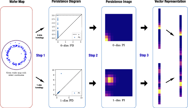
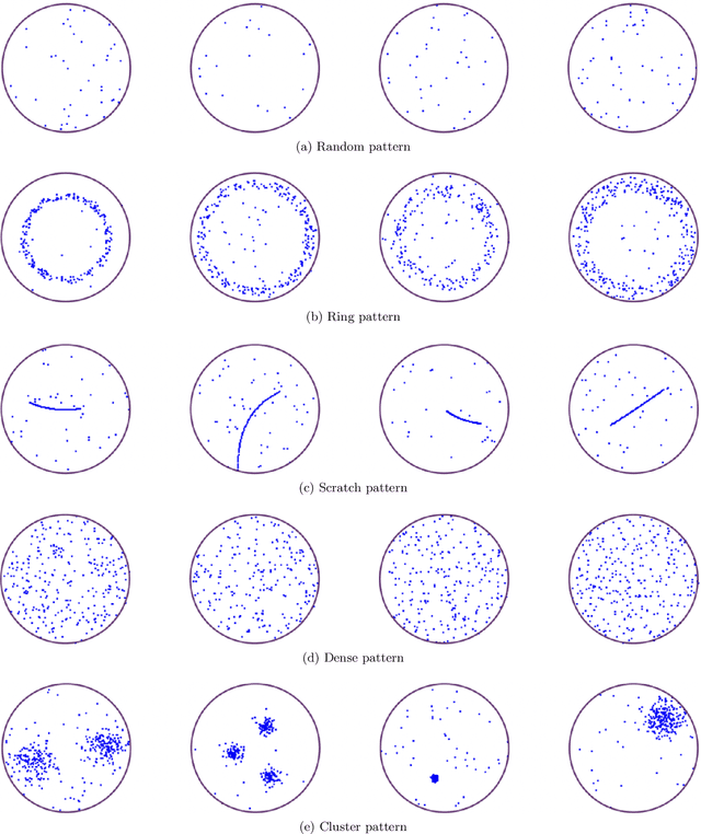
In semiconductor manufacturing, wafer map defect pattern provides critical information for facility maintenance and yield management, so the classification of defect patterns is one of the most important tasks in the manufacturing process. In this paper, we propose a novel way to represent the shape of the defect pattern as a finite-dimensional vector, which will be used as an input for a neural network algorithm for classification. The main idea is to extract the topological features of each pattern by using the theory of persistent homology from topological data analysis (TDA). Through some experiments with a simulated dataset, we show that the proposed method is faster and much more efficient in training with higher accuracy, compared with the method using convolutional neural networks (CNN) which is the most common approach for wafer map defect pattern classification. Moreover, our method outperforms the CNN-based method when the number of training data is not enough and is imbalanced.
 Add to Chrome
 Add to Firefox
 Add to Edge