Deep learning approach based on dimensionality reduction for designing electromagnetic nanostructures
Paper and Code
Feb 20, 2019


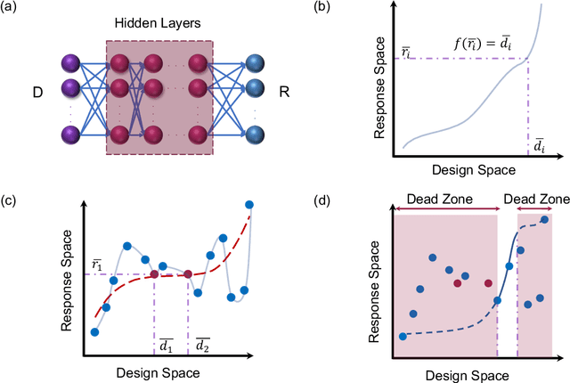
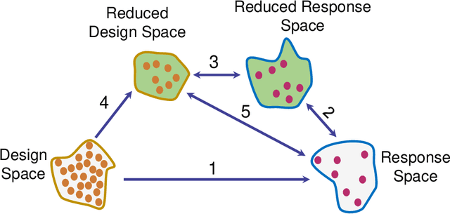
In this paper, we demonstrate a computationally efficient new approach based on deep learning (DL) techniques for analysis, design, and optimization of electromagnetic (EM) nanostructures. We use the strong correlation among features of a generic EM problem to considerably reduce the dimensionality of the problem and thus, the computational complexity, without imposing considerable errors. By employing the dimensionality reduction concept using the more recently demonstrated autoencoder technique, we redefine the conventional many-to-one design problem in EM nanostructures into a one-to-one problem plus a much simpler many-to-one problem, which can be simply solved using an analytic formulation. This approach reduces the computational complexity in solving both the forward problem (i.e., analysis) and the inverse problem (i.e., design) by orders of magnitude compared to conventional approaches. In addition, it provides analytic formulations that, despite their complexity, can be used to obtain intuitive understanding of the physics and dynamics of EM wave interaction with nanostructures with minimal computation requirements. As a proof-of-concept, we applied such an efficacious method to design a new class of on-demand reconfigurable optical metasurfaces based on phase-change materials (PCM). We envision that the integration of such a DL-based technique with full-wave commercial software packages offers a powerful toolkit to facilitate the analysis, design, and optimization of the EM nanostructures as well as explaining, understanding, and predicting the observed responses in such structures.
 Add to Chrome
 Add to Firefox
 Add to Edge