A CMOS SoC for Wireless Ultrasonic Power/Data Transfer and SHM Measurements on Structures
Paper and Code
Oct 24, 2021


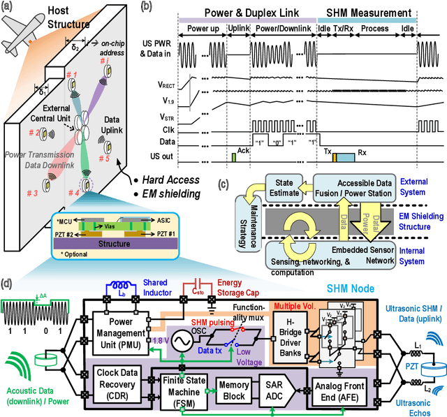
This paper describes a highly-integrated CMOS system-on-chip (SoC) for active structural health monitoring (SHM). The chip integrates ultrasonic power and bidirectional half-duplex data transfer, a power management unit (PMU), and an ultrasound transceiver to enable wireless ultrasonically-coupled sensor SHM networks on structures. The PMU includes an active bias-flip rectifier with off-delay compensation, high-efficiency dual-path DC-DC converter with inductor time-sharing, and five switched-capacitor DC-DC converters to generate multi-level spectrally band-limited pulses for guided-wave SHM. The chip was fabricated in a standard 180 nm process and has a die area of $2\times 2$ mm$^{2}$. Test results show power conversion efficiency (PCE) $>85\%$ for the active rectifier, $>70$\% for the inductive DC-DC converter, and $>60$\% for the switched-capacitor DC-DC converters. Output pulses have a peak-to-sidelobe ratio (PSL) $>30$~dB and worst-case out-of-band emissions $<-30$~dB, respectively. The SoC was integrated with a low-power microcontroller and passive components to realize miniaturized (15~mm $\times$ 30~mm) wireless SHM nodes. A set of nodes was deployed on an SHM test-bed (carbon fiber reinforced polymer sheet) representing an airframe panel. Tests on this wireless network confirm both long-range ultrasound power/data transfer and the ability to detect structural damage.
 Add to Chrome
 Add to Firefox
 Add to Edge